

Page 1
BB102M
Build in Biasing Circuit MOS FET IC
UHF RF Amplifier
Features
• Build in Biasing Circuit; To reduce using parts cost & PC board space.
• Low noise characteristics;
(NF = 2.1 dB typ. at f = 900 MHz)
• Withstanding to ESD;
Build in ESD absorbing diode. Withstand up to 200V at C=200pF, Rs=0 conditions.
• Provide mini mold packages; MPAK-4(SOT-143mod)
ADE-208-587 (Z)
1st. Edition
November 1997
Outline
MPAK-4
2
3
1
4
• Note 1 Marking is “BW–”.
• Note 2 BB302M is individual type number of HITACHI BBFET.
1. Source
2. Gate1
3. Gate2
4. Drain
Page 2
BB102M
Absolute Maximum Ratings (Ta = 25°C)
Item Symbol Ratings Unit
Drain to source voltage V
Gate1 to source voltage V
Gate2 to source voltage V
Drain current I
DS
G1S
G2S
D
Channel power dissipation Pch 150 mW
Channel temperature Tch 150 °C
Storage temperature Tstg –55 to +150 °C
Electrical Characteristics (Ta = 25°C)
Item Symbol Min Typ Max Unit Test Conditions
Drain to source breakdown
V
(BR)DSS
voltage
Gate1 to source breakdown
V
(BR)G1SS
voltage
Gate2 to source breakdown
V
(BR)G2SS
voltage
Gate1 to source cutoff current I
Gate2 to source cutoff current I
Gate1 to source cutoff voltage V
Gate2 to source cutoff voltage V
Drain current I
G1SS
G2SS
G1S(off)
G2S(off)
D(op)
Forward transfer admittance |yfs| 16 21 — mS VDS = 9V, VG1 = 9V, V
Input capacitance c
Output capacitance c
Reverse transfer capacitance c
iss
oss
rss
Power gain PG 16 20 — dB VDS = 9V, VG1 = 9V, V
Noise figure NF — 2.1 3.1 dB RG = 120kΩ, f = 900MHz
12 — — V ID = 200µA, V
+10 — — V IG1 = +10µA, V
±10 — — V IG2 = ±10µA, V
— — +100 nA V
——±100 nA V
0.1 — 0.8 V VDS = 9V, V
0.5 — 1.1 V VDS = 9V, V
10 15 20 mA VDS = 9V, VG1 = 9V, V
1.2 1.6 2.2 pF VDS = 9V, VG1 = 9V
0.7 1.1 1.5 pF V
— 0.011 0.03 pF f = 1MHz
12 V
+10
V
–0
±10 V
25 mA
= +9V, V
G1S
= ±9V, V
G2S
G2S
G1S
R
= 560kΩ
G
R
= 560kΩ, f = 1kHz
G
=6V, RG = 560kΩ
G2S
= V
G1S
G2S
= VDS = 0
G2S
= VDS = 0
G1S
= VDS = 0
G2S
= VDS = 0
G1S
= 6V, ID = 100µA
= 9V, ID = 100µA
G2S
G2S
G2S
= 0
= 6V
=6V
=6V
2
Page 3
Main Characteristics
BB102M
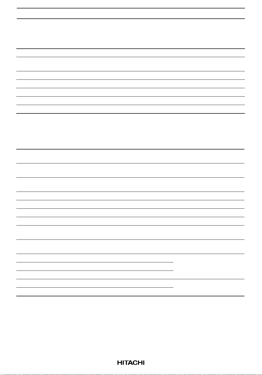
Test Circuit for Operating Items (I , |yfs|, Ciss, Coss, Crss, NF, PG)
V
G2 V
Gate 2
Drain
A
I
D
D(op)
Gate 1
Source
R
G
G1
Application Circuit
V = 6 to 0.3 V
AGC
BBFET
V = 9 V
DS
RFC
Output
Input
R
G
V = 9 V
GG
3
Page 4
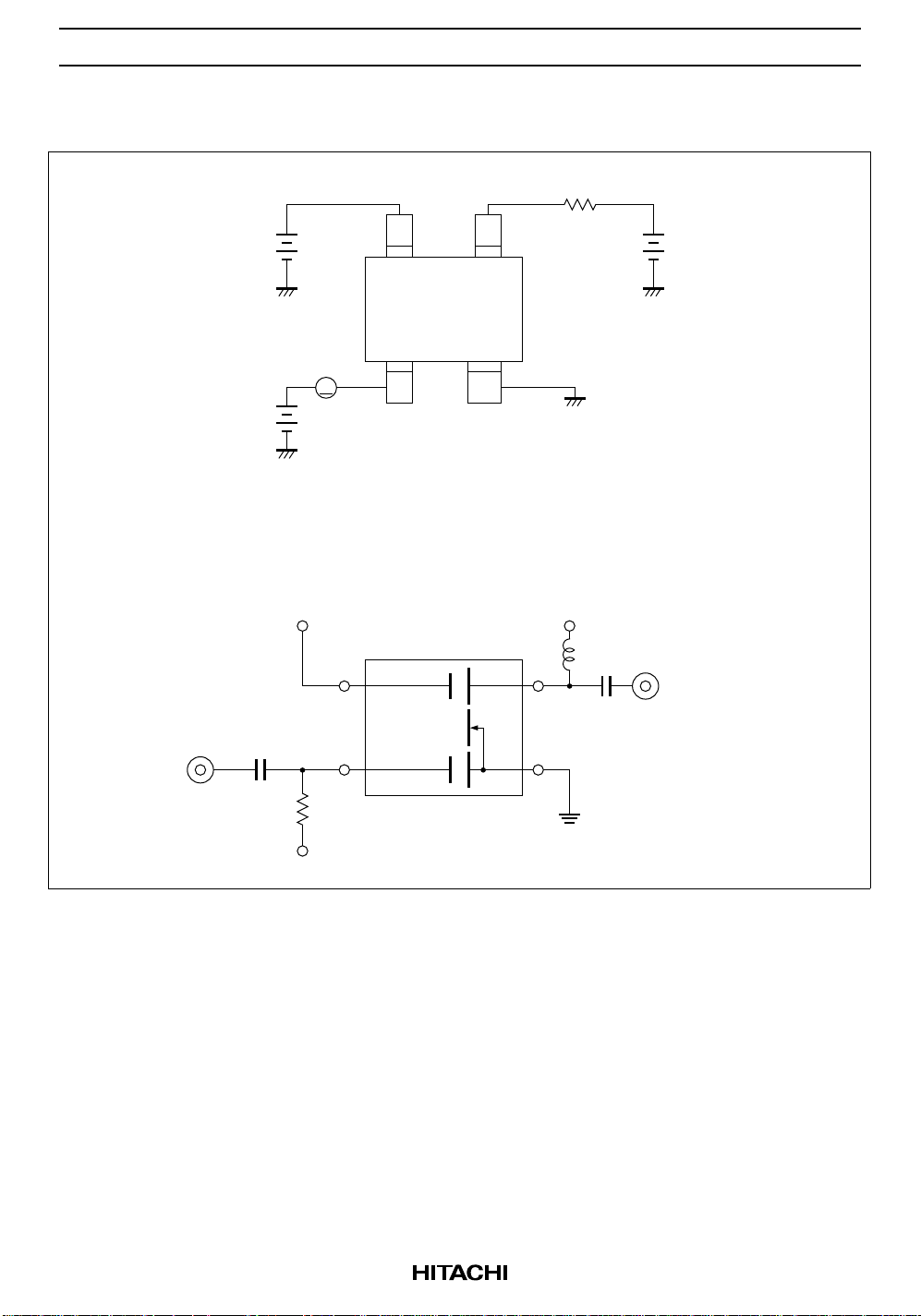
BB102M
200
150
100
50
Maximum Channel Power
Dissipation Curve
25
Typical Output Characteristics
V = 6 V
G2S
V = V
G1 DS
20
D
15
10
Drain Current I (mA)
5
Ω
Ω
270 k
330 k
390 k
470 k
560 k
680 k
820 k
1 MΩ
1.5 MΩ
R = 2.2 M
G
Ω
Ω
Ω
Ω
Ω
Ω
Channel Power Dissipation Pch (mW)
0
50 100 150 200
Ambient Temperature Ta (°C)
Drain Current vs.
Gate2 to Source Voltage
25
V = V = 9 V
20
D
15
10
DS
G1
270 k
330 k
390 k
Ω
Ω
470 k
560 k
680 k
820 k
1 MΩ
Ω
Ω
Ω
1.5 MΩ
Drain Current I (mA)
5
G
R = 2.2 M
0
246810
Drain to Source Voltage V (V)
DS
Drain Current vs. Gate1 Voltage
20
V = 9 V
DS
R = 470 k
G
16
D
12
Ω
Ω
Ω
6 V
5 V
4 V
3 V
2 V
8
Ω
Drain Current I (mA)
4
V = 1 V
G2S
0
1.2 2.4 3.8 4.8 6.0
Gate2 to Source Voltage V (V)
G2S
0
246810
Gate1 Voltage V (V)
G1
4
Page 5

BB102M
Drain Current vs. Gate1 Voltege
20
V = 9 V
DS
R = 560 k
16
D
G
Ω
12
8
Drain Current I (mA)
4
0
246810
Gate1 Voltage V (V)
Forward Transfer Admittance
vs. Gate1 Voltage
25
fs
20
15
6 V
5 V
4 V
3 V
2 V
V = 1 V
G2S
G1
6 V
5 V
4 V
3 V
2 V
Drain Current vs. Gate1 Voltege
20
V = 9 V
DS
R = 680 k
G
Ω
16
D
12
8
Drain Current I (mA)
4
0
246810
Gate1 Voltage V (V)
Forward Transfer Admittance
vs. Gate1 Voltage
25
fs
20
6 V
5 V
15
V = 1 V
G2S
G1
4 V
3 V
2 V
6 V
5 V
4 V
3 V
2 V
10
5
Forward Transfer Admittance |y | (mS)
0
246810
Gate1 Voltage V (V)
V = 9 V
DS
R = 470 k
G
f = 1 kHz
V = 1 V
G2S
G1
Ω
10
5
Forward Transfer Admittance |y | (mS)
0
246810
Gate1 Voltage V (V)
V = 9 V
DS
R = 560 k
G
f = 1 kHz
V = 1 V
G2S
G1
Ω
5
Page 6

BB102M
Forward Transfer Admittance
vs. Gate1 Voltage
25
fs
20
15
10
6 V
5 V
4 V
3 V
2 V
V = 9 V
DS
R = 680 k
G
f = 1 kHz
5
V = 1 V
Forward Transfer Admittance |y | (mS)
0
246810
Gate1 Voltage V (V)
G2S
G1
Power Gain vs. Gate Resistance
30
25
20
15
Ω
10
V = 9 V
V = 9 V
5
V = 6 V
f = 900 MHz
0
DS
G1
G2S
Power Gain PG (dB)Power Gain PG (dB)
10 20 50 100 200 500 1000
Gate Resistance R (k )
Ω
G
Noise Figure vs. Gate Resistance
4
V = 9 V
DS
V = 9 V
G1
V = 6 V
G2S
3
f = 900 MHz
2
1
Noise Figure NF (dB)
0
10 20 50 100 200 500 1000
Gate Resistance R (k )
Ω
G
30
25
20
15
10
5
0
Power Gain vs. Drain Current
V = 9 V
DS
V = 9 V
G1
V = 6 V
G2S
R = variable
G
f = 900 MHz
51015202530
Drain Current I (mA)
D
35 40
6
Page 7

BB102M
Noise Figure vs. Drain Current
4
3
2
V = 9 V
DS
V = 9 V
G1
1
Noise Figure NF (dB)
V = 6 V
G2S
R = variable
G
f = 900 MHz
0
5 10152025303540
Drain Current I (mA)
Gain Reduction vs.
Gate2 to Source Voltage
50
Drain Current vs. Gate Resistance
40
V = 9 V
DS
V = 9 V
G1
V = 6 V
30
D
G2S
20
10
Drain Current I (mA)
0
10 20 50 100 200 500 1000
D
Gate Resistance R (k )
Ω
G
Input Capacitance vs.
Gate2 to Source Voltage
3
40
V = 9 V
V = 9 V
V = 6 V
30
R = 560 k
f = 900 MHz
20
Gain Reduction GR (dB)
10
0
12345
Gate2 to Source Voltage V (V)
DS
G1
G2S
G
Ω
2
1
V = 9 V
DS
V = 9 V
Input Capacitance Ciss (pF)
G1
R = 560 k
G
Ω
f = 1 MHz
67 6
G2S
0
12345
Gate2 to Source Voltage V (V)
G2S
7
Page 8

BB102M
.4
.2
0
–.2
–.4
Test Condition :
150°
180°
–150°
Test Condition :
S11 Parameter vs. Frequency
1
.8
.6
.2
.6
.4
.8
–.6
–.8
–1
V = 9 V , V = 9 V
DS
V = 6 V , R = 560 k
G2S
1.5
2
1.5
234
1
–2
–1.5
G1
G
50 to 1000 MHz (50 MHz step)
S12 Parameter vs. Frequency
Scale: 0.01 / div.
90°
120°
–120°
–90°
V = 9 V , V = 9 V
DS
V = 6 V , R = 560 k
G2S
50 to 1000 MHz (50 MHz step)
60°
–60°
G1
G
S21 Parameter vs. Frequency
Scale: 1 / div.
90°
120°
3
4
5
10
10
5
–10
–5
–4
–3
Ω
150°
180°
–150°
Test Condition :
–120°
–90°
V = 9 V , V = 9 V
DS
V = 6 V , R = 560 k
G2S
–60°
G1
60°
G
30°
0°
–30°
Ω
50 to 1000 MHz (50 MHz step)
S22 Parameter vs. Frequency
1
30°
–30°
Ω
.8
.6
.4
.2
0°
0
–.2
.2
–.4
Test Condition :
.6
.4
.8
–.6
–.8
–1
V = 9 V , V = 9 V
DS
V = 6 V , R = 560 k
G2S
50 to 1000 MHz (50 MHz step)
1.5
2
3
4
5
10
1.5
234
1
–1.5
G1
10
5
–10
–5
–4
–3
–2
G
Ω
8
Page 9

BB102M
Sparameter (VDS = VG1 = 9V, V
S11 S21 S12 S22
f (MHz) MAG ANG MAG ANG MAG ANG MAG ANG
50 0.995 –2.9 2.22 176.0 0.00046 66.9 0.977 –1.0
100 0.991 –6.0 2.21 172.0 0.00109 90.4 0.987 –3.2
150 0.987 –9.4 2.21 168.0 0.00122 76.5 0.987 –5.0
200 0.985 –12.4 2.19 163.6 0.00180 81.9 0.985 –6.7
250 0.975 –15.4 2.18 159.3 0.00228 86.0 0.983 –8.4
300 0.969 –18.4 2.15 155.3 0.00246 78.8 0.981 –10.0
350 0.954 –21.5 2.12 151.7 0.00273 76.2 0.979 –11.7
400 0.948 –24.6 2.11 147.6 0.00331 66.9 0.976 –13.4
450 0.933 –27.5 2.08 143.7 0.00334 74.7 0.973 –14.9
500 0.923 –30.7 2.05 139.9 0.00357 68.4 0.969 –16.8
550 0.912 –33.6 2.02 136.2 0.00328 67.5 0.965 –18.3
600 0.892 –36.3 1.99 123.9 0.00305 69.8 0.961 –19.9
650 0.882 –39.3 1.96 128.7 0.00322 66.7 0.958 –21.5
700 0.868 –42.0 1.92 125.4 0.00297 70.3 0.953 –23.4
750 0851 –45.0 1.90 122.0 0.00286 74.4 0.948 –24.7
800 0.834 –47.7 1.87 117.9 0.00273 71.9 0.944 –26.2
850 0.815 –50.6 1.83 114.9 0.00226 88.1 0.940 –27.9
900 0.801 –53.5 1.82 111.2 0.00143 95.5 0.934 –29.4
950 0.788 –55.9 1.79 107.8 0.00131 98.6 0.931 –31.0
1000 0.768 –58.5 1.77 104.4 0.00189 145.2 0.925 –32.9
= 6V, RG = 560kΩ, Zo = 50Ω)
G2S
9
Page 10

BB102M
Package Dimensions
2.8
1.9
0.95 0.95
3
0.4
+ 0.1
– 0.05
+ 0.3
– 0.1
Unit: mm
+ 0.1
– 0.3
+ 0.1
0.4
– 0.05
0.65
2
0.16
+ 0.1
– 0.06
0.4
+ 0.1
– 0.05
+ 0.2
– 0.6
1.5
2.8
0.85
1
+ 0.1
0.6
– 0.05
+ 0.1
– 0.3
0.65
4
0.95
0 ~ 0.1
1.8
0.3
+ 0.2
– 0.1
1.1
Hitachi Code
EIAJ
JEDEC
MPAK–4
SC–61AA
—
10
Page 11

Cautions
1. Hitachi neither warrants nor grants licenses of any rights of Hitachi’s or any third party’s patent,
copyright, trademark, or other intellectual property rights for information contained in this document.
Hitachi bears no responsibility for problems that may arise with third party’s rights, including
intellectual property rights, in connection with use of the information contained in this document.
2. Products and product specifications may be subject to change without notice. Confirm that you have
received the latest product standards or specifications before final design, purchase or use.
3. Hitachi makes every attempt to ensure that its products are of high quality and reliability. However,
contact Hitachi’s sales office before using the product in an application that demands especially high
quality and reliability or where its failure or malfunction may directly threaten human life or cause risk
of bodily injury, such as aerospace, aeronautics, nuclear power, combustion control, transportation,
traffic, safety equipment or medical equipment for life support.
4. Design your application so that the product is used within the ranges guaranteed by Hitachi particularly
for maximum rating, operating supply voltage range, heat radiation characteristics, installation
conditions and other characteristics. Hitachi bears no responsibility for failure or damage when used
beyond the guaranteed ranges. Even within the guaranteed ranges, consider normally foreseeable
failure rates or failure modes in semiconductor devices and employ systemic measures such as failsafes, so that the equipment incorporating Hitachi product does not cause bodily injury, fire or other
consequential damage due to operation of the Hitachi product.
5. This product is not designed to be radiation resistant.
6. No one is permitted to reproduce or duplicate, in any form, the whole or part of this document without
written approval from Hitachi.
7. Contact Hitachi’s sales office for any questions regarding this document or Hitachi semiconductor
products.
Hitachi, Ltd.
Semiconductor & Integrated Circuits.
Nippon Bldg., 2-6-2, Ohte-machi, Chiyoda-ku, Tokyo 100-0004, Japan
Tel: Tokyo (03) 3270-2111 Fax: (03) 3270-5109
URL NorthAmerica : http:semiconductor.hitachi.com/
For further information write to:
Hitachi Semiconductor
(America) Inc.
179 East Tasman Drive,
San Jose,CA 95134
Tel: <1> (408) 433-1990
Fax: <1>(408) 433-0223
Europe : http://www.hitachi-eu.com/hel/ecg
Asia (Singapore) : http://www.has.hitachi.com.sg/grp3/sicd/index.htm
Asia (Taiwan) : http://www.hitachi.com.tw/E/Product/SICD_Frame.htm
Asia (HongKong) : http://www.hitachi.com.hk/eng/bo/grp3/index.htm
Japan : http://www.hitachi.co.jp/Sicd/indx.htm
Hitachi Europe GmbH
Electronic components Group
Dornacher Stra§e 3
D-85622 Feldkirchen, Munich
Germany
Tel: <49> (89) 9 9180-0
Fax: <49> (89) 9 29 30 00
Hitachi Europe Ltd.
Electronic Components Group.
Whitebrook Park
Lower Cookham Road
Maidenhead
Berkshire SL6 8YA, United Kingdom
Tel: <44> (1628) 585000
Fax: <44> (1628) 778322
Hitachi Asia Pte. Ltd.
16 Collyer Quay #20-00
Hitachi Tower
Singapore 049318
Tel: 535-2100
Fax: 535-1533
Hitachi Asia Ltd.
Taipei Branch Office
3F, Hung Kuo Building. No.167,
Tun-Hwa North Road, Taipei (105)
Tel: <886> (2) 2718-3666
Fax: <886> (2) 2718-8180
Copyright ' Hitachi, Ltd., 1999. All rights reserved. Printed in Japan.
Hitachi Asia (Hong Kong) Ltd.
Group III (Electronic Components)
7/F., North Tower, World Finance Centre,
Harbour City, Canton Road, Tsim Sha Tsui,
Kowloon, Hong Kong
Tel: <852> (2) 735 9218
Fax: <852> (2) 730 0281
Telex: 40815 HITEC HX
 Loading...