

Page 1
DATA SH EET
Product specification
Supersedes data of April 1996
1996 Sep 17
DISCRETE SEMICONDUCTORS
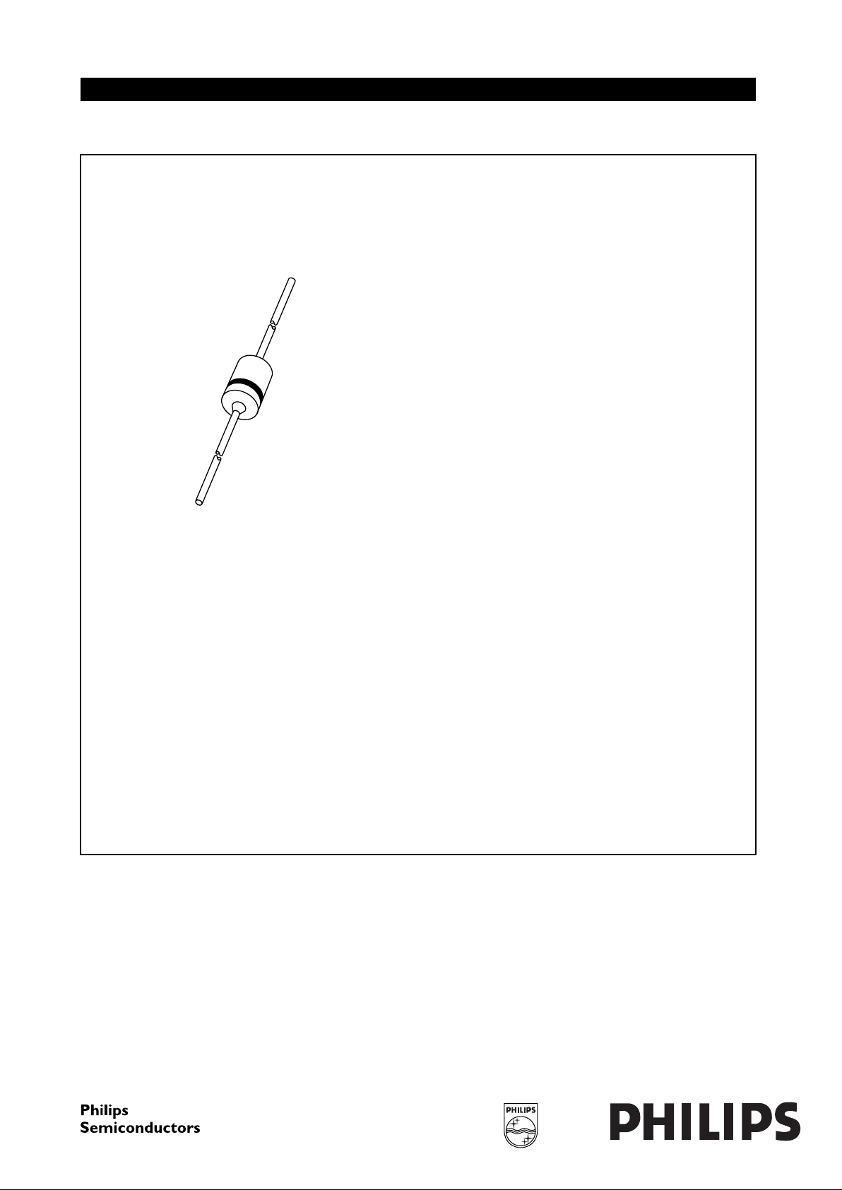
BAX12
Controlled avalanche diode
M3D176
Page 2
1996 Sep 17 2
Philips Semiconductors Product specification
Controlled avalanche diode BAX12
FEATURES
• Hermetically sealed leaded glass
SOD27 (DO-35) package
• Switching speed: max. 50 ns
• General application
• Continuous reverse voltage:
max. 90 V
• Repetitive peak reverse voltage:
max. 90 V
• Repetitive peak forward current:
max. 800 mA
• Repetitive peak reverse current:
max. 600 mA
• Capable of absorbing transients
repetitively.
APPLICATIONS
• Switching of inductive loads in
semi-electronic telephone
exchanges.
DESCRIPTION
The BAX12 is a controlled avalanche diode fabricated in planar technology, and
encapsulated in the hermetically sealed leaded glass SOD27 (DO-35)
package.
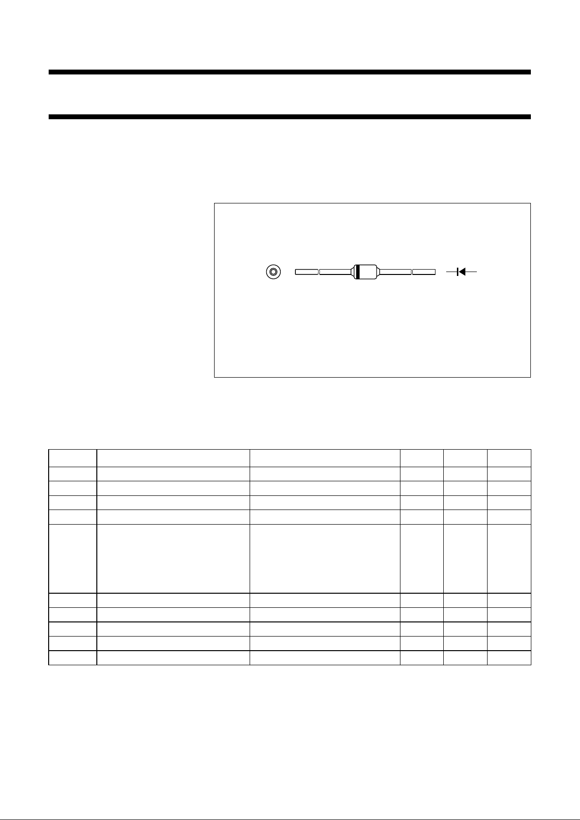
Fig.1 Simplified outline (SOD27; DO35) and symbol.
Marking code: BAX12.
handbook, halfpage
MAM246
k
a
LIMITING VALUES
In accordance with the Absolute Maximum Rating System (IEC 134).
Notes
1. It is allowed to exceed this value; see Figs 8 and 9. Care should be taken not to exceed the I
RRM
rating.
2. Device mounted on an FR4 printed circuit-board; lead length 10 mm.
SYMBOL PARAMETER CONDITIONS MIN. MAX. UNIT
V
RRM
repetitive peak reverse voltage note 1 − 90 V
V
R
continuous reverse voltage note 1 − 90 V
I
F
continuous forward current see Fig.2; note 2 − 400 mA
I
FRM
repetitive peak forward current − 800 mA
I
FSM
non-repetitive peak forward current square wave; Tj=25°C prior to
surge; see Fig.4
t=1µs − 55 A
t = 100 µs − 15 A
t = 10 ms − 9A
P
tot
total power dissipation T
amb
=25°C; note 2 − 450 mW
I
RRM
repetitive peak reverse current − 600 mA
E
RRM
repetitive peak reverse energy tp≥ 50 µs; f ≤ 20 Hz; Tj=25°C − 5.0 mJ
T
stg
storage temperature −65 +200 °C
T
j
junction temperature − 200 °C
Page 3

1996 Sep 17 3
Philips Semiconductors Product specification
Controlled avalanche diode BAX12
ELECTRICAL CHARACTERISTICS
T
j
=25°C; unless otherwise specified.
THERMAL CHARACTERISTICS
Note
1. Device mounted on a printed circuit-board without metallization pad.
SYMBOL PARAMETER CONDITIONS MIN. MAX. UNIT
V
F
forward voltage see Fig.3
I
F
=10mA − 750 mV
I
F
=50mA − 840 mV
I
F
= 100 mA − 900 mV
I
F
= 200 mA − 1.0 V
I
F
= 400 mA − 1.25 V
I
R
reverse current see Fig.5
V
R
=90V − 100 nA
V
R
= 90 V; Tj= 150 °C − 100 µA
V
(BR)R
reverse avalanche breakdown voltage IR= 1 mA 120 170 V
C
d
diode capacitance f = 1 MHz; VR=0;
see Fig.6
− 35 pF
t
rr
reverse recovery time when switched from
IF= 30 mA to IR=30mA;
RL= 100 Ω; measured at
IR= 3 mA; see Fig.10
− 50 ns
SYMBOL PARAMETER CONDITIONS VALUE UNIT
R
th j-tp
thermal resistance from junction to tie-point lead length 10 mm 240 K/W
R
th j-a
thermal resistance from junction to ambient lead length 10 mm; note 1 375 K/W
Page 4

1996 Sep 17 4
Philips Semiconductors Product specification
Controlled avalanche diode BAX12
GRAPHICAL DATA
Fig.2 Maximum permissible continuous forward
current as a function of ambient
temperature.
handbook, halfpage
0 100 200
400
500
300
200
0
100
MBG455
T
amb
(oC)
I
F
(mA)
Device mounted on an FR4 printed-circuit board; lead length 10 mm.
Fig.3 Forward current as a function of forward
voltage.
handbook, halfpage
012
600
0
200
400
MBG463
VF (V)
I
F
(mA)
(1) (2) (3)
(1) Tj= 175 °C; typical values.
(2) Tj=25°C; typical values.
(3) Tj=25°C; maximum values.
Fig.4 Maximum permissible non-repetitive peak forward current as a function of pulse duration.
Based on square wave currents.
Tj=25°C prior to surge.
handbook, full pagewidth
MBG702
10
tp (µs)
1
I
FSM
(A)
10
2
10
−1
10
4
10
2
10
3
10
1
Page 5

1996 Sep 17 5
Philips Semiconductors Product specification
Controlled avalanche diode BAX12
Fig.5 Reverse current as a function of junction temperature.
handbook, full pagewidth
0 100 200
10
10
2
10
4
10
3
10
5
10
6
10
7
MBG696
I
R
(nA)
T
j
(
o
C)
VR=90V.
Solid line; maximum values. Dotted line; typical values.
Fig.6 Diode capacitance as a function of reverse
voltage; typical values.
f = 1 MHz; Tj=25°C.
handbook, halfpage
0102030
V
R
(V)
40
C
d
(pF)
30
10
0
20
MGD003
Fig.7 Maximum permissible repetitive peak
reverse power as a function of the pulse
duration T ≥ 50 ms; Tj=25°C.
Solid line; rectangular waveform; δ≤0.01.
Dotted line; triangular waveform; δ≤0.02.
(1) Limited by I
RMM
= 600 mA.
handbook, half age
MBG701
10
−1
110
1
10
10
2
10
3
10
−2
P
RRM
(W)
t (ms)
(1)
Page 6

1996 Sep 17 6
Philips Semiconductors Product specification
Controlled avalanche diode BAX12
Fig.8 Reverse current as a function of continuous
reverse voltage.
handbook, halfpage
100 200
600
0
200
400
MBG698
150
(1) (4)
I
R
(mA)
VR (V)
(2) (3)
Reverse voltages higher than the VR ratings are allowed, provided:
a. The transient energy ≤ 7.5 mJ at P
RRM
≤30 W; Tj=25°C;
the transient energy ≤ 5 mJ at P
RRM
= 120 W; Tj=25°C (see Fig.7).
b. T ≥ 50 ms; δ≤0.01 (rectangular waveform) (see Fig.9).
δ≤0.02 (triangular waveform) (see Fig.9).
With increasing temperature, the maximum permissible transient
energy must be decreased by 0.03 mJ/K.
(1) T
j
=25°C; minimum values.
(2) Tj= 175 °C; minimum values.
(3) Tj=25°C; maximum values.
(4) Tj= 175 °C; maximum values.
Fig.9 Peak reverse voltage and current test
pulses.
handbook, halfpage
MBG699
V
R
I
R
T
time
time
t (rectangular waveform)
t
(triangular
waveform)
δ =
t
T
Page 7

1996 Sep 17 7
Philips Semiconductors Product specification
Controlled avalanche diode BAX12
Fig.10 Reverse recovery voltage test circuit and waveforms.
Input signal: reverse pulse rise time tr= 0.6 ns; reverse pulse duration tp= 100 ns; duty factor δ = 0.05.
Oscilloscope: rise time tr= 0.35 ns.
Circuit capacitance: C ≤ 1 pF (oscilloscope input capacitance + parasitic capacitance).
(1) IR= 3 mA.
handbook, full pagewidth
t
rr
(1)
I
F
t
output signal
t
r
t
t
p
10%
90%
V
R
input signal
V = V I x R
RF S
R = 50SΩ
I
F
D.U.T.
R = 50iΩ
SAMPLING
OSCILLOSCOPE
MGA881
Page 8

1996 Sep 17 8
Philips Semiconductors Product specification
Controlled avalanche diode BAX12
PACKAGE OUTLINE
DEFINITIONS
LIFE SUPPORT APPLICATIONS
These products are not designed for use in life support appliances, devices, or systems where malfunction of these
products can reasonably be expected to result in personal injury. Philips customers using or selling these products for
use in such applications do so at their own risk and agree to fully indemnify Philips for any damages resulting from such
improper use or sale.
Data Sheet Status
Objective specification This data sheet contains target or goal specifications for product development.
Preliminary specification This data sheet contains preliminary data; supplementary data may be published later.
Product specification This data sheet contains final product specifications.
Limiting values
Limiting values given are in accordance with the Absolute Maximum Rating System (IEC 134). Stress above one or
more of the limiting values may cause permanent damage to the device. These are stress ratings only and operation
of the device at these or at any other conditions above those given in the Characteristics sections of the specification
is not implied. Exposure to limiting values for extended periods may affect device reliability.
Application information
Where application information is given, it is advisory and does not form part of the specification.
Fig.11 SOD27 (DO-35).
Dimensions in mm.
dbook, full pagewidth
MLA428 - 1
25.4 min
4.25
max
1.85
max
25.4 min
0.56
max
 Loading...