

Page 1
Rev. A/NX
BAW56WS
Page 1 of 6
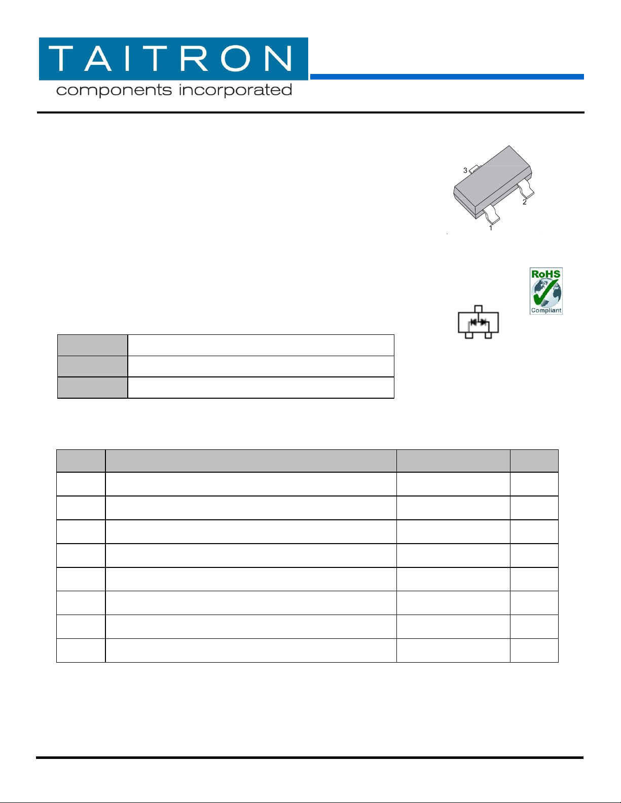
Three Terminals
SMD Switching Diode
Symbol
Description
BAW56
Unit
Marking Code
JC
VRM
Reverse Voltage
75
V
VRRM
Peak Reverse Voltage
100
V
IF(AV)
Forward Average Current, Half Wave Rectification with Resistive
Load and f≥50Hz
150
mA
IFSM
Peak Forward Surge Current (0.001mS)
4
A
PD
Power Dissipation Derate above 25° C
200
mW
TJ
Junction Temperature
-55 to +150
° C
TSTG
Storage Temperature Range
-55 to +150
° C
Case:
SOT-323, Plastic Case
Terminals:
Solderable per MIL-STD-750, Method 2026
Weight:
Approx. 0.005 gram
SOT-323
Three Terminals SMD Switching Diode
Features
Fast switching speed
Surface mount package ideally suited for automatic insertion
Electrically Identical to Standard JEDEC
High Conductance
RoHS Compliant
Mechanical Data
Maximum Ratings (T
=25ºC unless noted otherwise)
Ambient
Page 2
Three Terminals SMD Switching Diode
Rev. A/NX
BAW56WS
www.taitroncomponents.com
Page 2 of 6
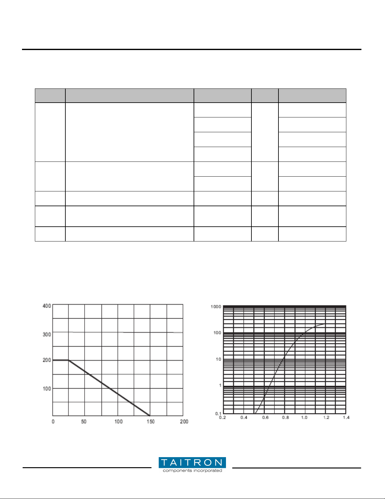
Fig.1- Power Derating Curve
Fig.2- Typical Forward Characteristics
Ambient Temperature (°C )
Forward Voltage (V)
Symbol
Description
BAW56
Unit
Conditions
VF
Forward Voltage
0.715
V
IF=1mA
0.855
IF=10mA
1.0
IF=50mA
1.25
IF=150mA
IR
Reverse Current
0.03
µA
VR=25V
2.5
VR=75V
CT
Total Capacitance
1.5
pF
VR=0V, f=1MHz
Trr
Reverse Recovery Time
4
nS
From IF=10mA to
IR=1mA, VR=6V
RL=100Ω
RthJA
Thermal Resistance from Junction to Ambient
Air
625
° C/W
Forward Current (mA)
Power Dissipation (mW)
Electrical Characteristics (T
=25ºC unless noted otherwise)
Ambient
Typical Characteristics Curves
Page 3
Three Terminals SMD Switching Diode
Rev. A/NX
BAW56WS
www.taitroncomponents.com
Page 3 of 6
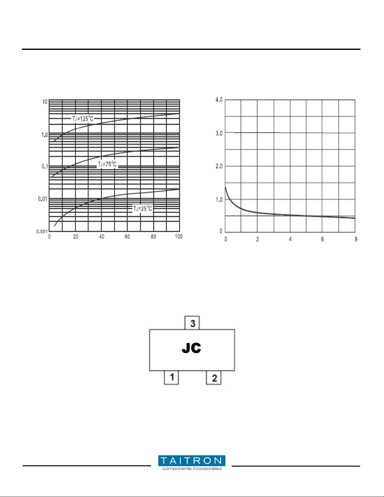
Fig.3- Typical Reverse Characteristics
Reverse Voltage (V)
Reverse Current (µA)
Fig.4- Typical Junction Capacitance
Reverse Voltage (V)
Junction Capacitance (pF)
Marking Information:
Page 4

Three Terminals SMD Switching Diode
Rev. A/NX
BAW56WS
www.taitroncomponents.com
Page 4 of 6
SOT-323
Dimensions in inch (mm)
Page 5

Three Terminals SMD Switching Diode
Rev. A/NX
BAW56WS
www.taitroncomponents.com
Page 5 of 6
Product Type
A0
B0
K0 D P0
P
See Note
1.55±0.5
4.0±0.1
4.0±0.1
SOT-323
W
E T D1
F
P2
8.0+0.3/-0.1
1.75±0.1
0.38±0.1
1.0±0.05
3.5±0.5
2.0±0.05
A C G
T
178.0±2.0
13.0±0.5
8.4±2.0
14.4 max.
Packing Information:
Carrier Tape Dimensions (in mm)
Note: Symbol A0, B0, K0 are determined by the maximum dimensions of the component size.
The clearance between the component and the cavity must be within
0.05 mm (0.002’’) min. to 0.50 mm (0.02’’) max. for 8 mm tape.
Reel Dimensions (in mm)
Page 6

Three Terminals SMD Switching Diode
Rev. A/NX
BAW56WS
www.taitroncomponents.com
Page 6 of 6
Quantity
PCS per Inner Box
PCS per Inner Carton
TR70 Tape & Reel
3000/Reel
240000
Cartoon Size
390X270X400 (in mm)
US HEADQUARTERS
28040 WEST HARRISON PARKWAY, VALENCIA, CA 91355-4162
Tel: (800) TAITRON (800) 824-8766 (661) 257-6060
Fax: (800) TAITFAX (800) 824-8329 (661) 257-6415
Email: taitron@taitroncomponents.com
Http://www.taitroncomponents.com
TAITRON COMPONENTS MEXICO, S.A .DE C.V.
BOULEVARD CENTRAL 5000 INTERIOR 5 PARQUE INDUSTRIAL ATITALAQUIA, HIDALGO C.P. 42970
MEXICO
Tel: +52-55-5560-1519
Fax: +52-55-5560-2190
TAITRON COMPONENTS INCORPORATED REPRESENTAÇÕES DO BRASIL LTDA
RUA DOMINGOS DE MORAIS, 2777, 2.ANDAR, SALA 24 SAÚDE - SÃO PAULO-SP 04035-001 BRAZIL
Tel: +55-11-5574-7949
Fax: +55-11-5572-0052
TAITRON COMPONENTS INCORPORATED, SHANGHAI REPRESENTATIVE OFFICE
METROBANK PLAZA, 1160 WEST YAN’ AN ROAD, SUITE 1503, SHANGHAI, 200052, CHINA
Tel: +86-21-5424-9942
Fax: +86-21-5424-9931
Packing Quantity Information:
Inner Carton Size Information:
How to contact us:
Page 7

 Loading...