

Page 1
1/5
BAT60J
May 2000 - Ed: 4A
SMALL SIGNAL SCHOTTKY DIODE
n VERY SMALL CONDUCTION LOSSES
n NEGLIGIBLE SWITCHING LOSSES
n LOW FORWARDVOLTAGE DROP
n EXTREMELY FAST SWITCHING
n SURFACE MOUNTED DEVICE
FEATURES AND BENEFITS
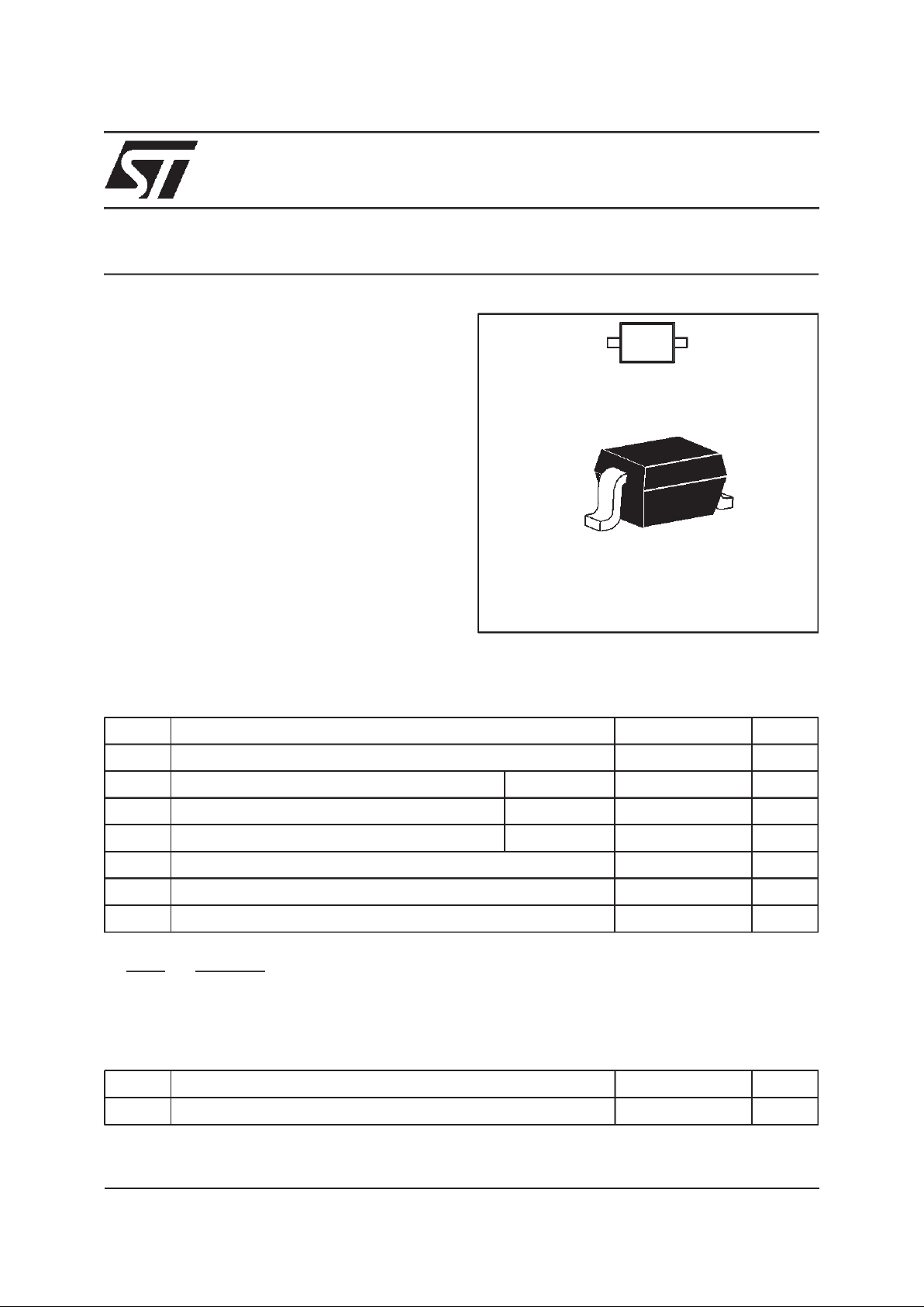
Schottky barrierdiode encapsulated in aSOD-323
small SMD package.
This device is intended for use in portable
equipments. It is suited for DC to DC converters,
step-up conversionand power management.
DESCRIPTION
SOD-323
Symbol Parameter Value Unit
V
RRM
Repetitive peak reverse voltage 10 V
I
F
Peak forward current δ = 0.11 3 A
I
FSM
Surge non repetitive forward current tp=10ms 5 A
P
tot
Power Dissipation Ta=25°C 310 mW
T
stg
Storage temperature range - 65 to +150 °C
Tj Maximum operatingjunction temperature * 150 °C
TL Maximum temperaturefor soldering during 10s 260 °C
ABSOLUTE RATINGS (limiting values)
Symbol Parameter Value Unit
R
th (j-a)
Junction to ambient (*) 400 °C/W
(*) Mounted onepoxy board with recommended padlayout.
THERMAL RESISTANCE
*:
dPtot
dTj Rth j a
<
−1()
thermal runaway condition for a diode on its own heatsink
A
K
60
Page 2

BAT60J
2/5
Symbol Tests Conditions Tests conditions Min. Typ. Max. Unit
VF* Forward voltage drop Tj = 25°CI
F
= 10 mA 0.28 0.32 V
IF= 100 mA 0.35 0.40
IF= 1 A 0.53 0.58
IR** Reverseleakage current Tj = 25°CV
R
=5V 1 3 µA
Tj = 25°CV
R
= 8 V 1.3 4
Tj = 80°CV
R
= 8 V 73 150
STATIC ELECTRICAL CHARACTERISTICS
Pulse test: * tp = 380µs, δ <2%
** tp = 5ms, δ <2%
To evaluate the conduction losses the following equation:
P = 0.38 x I
F(AV)
+ 0.17 I
F2(RMS)
Page 3

BAT60J
3/5
0.0 0.1 0.2 0.3 0.4 0.5 0.6 0.7
0.00
0.05
0.10
0.15
0.20
0.25
0.30
0.35
IF(av) (A)
PF(av)(W)
T
δ
=tp/T
tp
δ = 0.05
δ = 0.1
δ = 0.2
δ = 0.5
δ =1
Fig. 1: Average forward power dissipation versus
average forward current.
0 25 50 75 100 125 150
0.0
0.4
0.8
1.2
1.6
2.0
2.4
2.8
3.2
Tamb(°C)
IF(A)
T
δ
=tp/T
tp
Fig. 2-1: Peak forward current versus ambient
temperature (δ = 0.11).
0 25 50 75 100 125 150
0.00
0.05
0.10
0.15
0.20
0.25
0.30
0.35
0.40
0.45
0.50
0.55
0.60
Tamb(°C)
IF(av)(A)
T
δ
=tp/T
tp
Fig. 2-2: Average forward current versus ambient
temperature (δ = 0.5).
1E-3 1E-2 1E-1 1E+0
0.0
0.5
1.0
1.5
2.0
2.5
3.0
t(s)
IM(A)
Ta=25°C
Ta=50°C
Ta=75°C
IM
t
δ=0.5
Fig. 3: Non repetitive surge peakforward current
versus overload duration (maximum values).
1E-4 1E-3 1E-2 1E-1 1E+0 1E+1 1E+2
1E-3
1E-2
1E-1
1E+0
t(s)
Zth(j-a)/Rth(j-a)
δ =0.5
δ =0.2
δ = 0.1
Single pulse
T
δ
=tp/T tp
Fig.4:Relative variation of thermal impedance junctionto ambient versuspulseduration (Epoxy printed
circuit boardFR4 with recommended padlayout).
012345678910
1E-4
1E-3
1E-2
1E-1
1E+0
1E+1
VR(V)
IR(mA)
Tj=80°C
Tj=25°C
Tj=150°C
Fig.5: Reverseleackage current versus reverse
voltageapplied (typical values).
Page 4

BAT60J
4/5
0 25 50 75 100 125 150
1E-1
1E+0
1E+1
1E+2
1E+3
1E+4
1E+5
Tj(°C)
IR[Tj] / IR[Tj=25°C]
VR=8V
Fig.6: Reverseleackage current versus junction
temperature(typical values).
110
10
100
VR(V)
C(pF)
F=1MHz
Tj=25°C
Fig.7:Junction capacitance versus reverse voltage
applied (typicalvalues).
0.0 0.2 0.4 0.6 0.8 1.0 1.2 1.4 1.6 1.8
1E-1
1E+0
1E+1
VFM(V)
IFM(A)
Tj=150°C
(Typicalvalues)
Tj=80°C
(Typicalvalues)
Tj=25°C
(Maximumvalues)
Fig.8-1:Forwardvoltagedropversusforwardcurrent(Highlevel).
0.0 0.1 0.2 0.3 0.4 0.5 0.6 0.7 0.8
0.0
0.1
0.2
0.3
0.4
0.5
0.6
0.7
0.8
0.9
1.0
VFM(V)
IFM(A)
Tj=150°C
(Typicalvalues)
Tj=25°C
(Maximumvalues)
Tj=80°C
(Typicalvalues)
Fig.8-2: Forwardvoltagedropversusforwardcurrent(Lowlevel).
0 102030405060708090100
100
150
200
250
300
350
400
450
500
550
600
S(Cu) (mm )
Rth(j-a) (°C/W)
IF=0.75A
Fig.9:Thermal resistance junction to ambient versuscopper surface (epoxyprinted circuitboard FR4,
copper thickness: 35µm).
Page 5

BAT60J
5/5
Information furnished isbelieved to beaccurate and reliable. However, STMicroelectronics assumes no responsibility for theconsequences of
use of such information nor forany infringementof patents or other rightsof third parties which may result from its use.No license is granted by
implication or otherwise under any patent or patent rights of STMicroelectronics. Specifications mentioned in this publication are subject to
change without notice. This publication supersedes and replaces all information previously supplied.
STMicroelectronics products are not authorized for use as critical components in life support devices or systems without express written approval of STMicroelectronics.
The ST logo is a registered trademark of STMicroelectronics
2000 STMicroelectronics - Printed in Italy - All rights reserved.
STMicroelectronics GROUP OF COMPANIES
Australia - Brazil - China - Finland - France - Germany - Hong Kong - India - Italy - Japan - Malaysia
Malta - Morocco - Singapore - Spain - Sweden - Switzerland - United Kingdom - U.S.A.
http://www.st.com
PACKAGE MECHANICAL DATA
SOD-323
H
b
D
E
A1
A
L
Q1
c
REF.
DIMENSIONS
Millimeters Inches
Min. Max. Min. Max.
A 1.17 0.046
A1 0 0.1 0 0.004
b 0.25 0.44 0.01 0.017
c 0.1 0.25 0.004 0.01
D 1.52 1.8 0.06 0.071
E 1.11 1.45 0.044 0.057
H 2.3 2.7 0.09 0.106
L 0.1 0.46 0.004 0.02
Q1 0.1 0.41 0.004 0.016
Type Marking Package Weight Base qty Delivery mode
BAT60J 60 SOD-323 0.005 g. 3000 Tape & reel
n Epoxy meets UL94V-0
MARKING
 Loading...