

Datasheet BAS70-05FILM, BAS70-04FILM, BAS70-06FILM, BAR18FILM Datasheet (SGS Thomson Microelectronics)
Page 1
1/4
®
BAR 18
BAS70-04 06
SMALL SIGNAL SCHOTTKY DIODES
December 2001 - Ed: 3A
Symbol Parameter Value Unit
V
RRM
Repetitive peak reverse voltage
70 V
I
F
Continuous forward current
70 mA
P
tot
Power dissipation (note 1) Tamb = 25°C
250 mW
T
stg
Maximum storage temperature range
- 65 to +150 °C
Tj
Maximum operating junction temperature *
150
°C
T
L
Maximum temperature for soldering during 10s
260
°C
Note 1: for double diodes, Ptot is the total dissipation of both diodes
ABSOLUTE RATINGS (limiting values)
Symbol Parameter Value Unit
R
th (j-a)
Junction to ambient (*)
500 °C/W
(*) Mounted on epoxy board with recommended pad layout.
THERMAL RESISTANCE
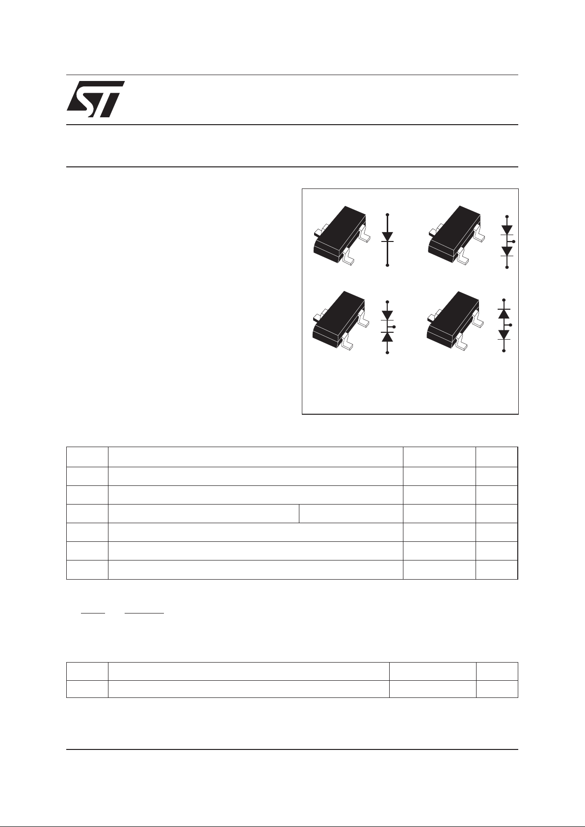
SOT-23
(Plastic)
K
N.C.
A
BAR18
A
K1
K2
BAS70-06
K
A1
A2
BAS70-05
A1
K2
K1
A2
BAS70-04
* :
dPtot
dTj Rth j a
<
−1()
thermal runaway condition for a diode on its own heatsink
Lowturn-onandhighbreakdownvoltagediodesintendedfor ultrafast switching and UHF detectors in
hybrid micro circuits.
DESCRIPTION
Page 2
BAR 18 / BAS70-04 06
2/4
Symbol Test Conditions Min. Typ. Max. Unit
V
BR
Tj = 25°C IR= 10µA
70 V
VF*
Tj = 25°C IF= 1mA
410 mV
I
R
**
Tj = 25°C VR= 50V
200 nA
STATIC CHARACTERISTICS
ELECTRICAL CHARACTERISTICS
Symbol Test Conditions Min. Typ. Max. Unit
C
Tj = 25°C VR= 0V F = 1MHz
2pF
τ*
Tj = 25°C IF= 5mA Krakauer Method
100 ps
DYNAMIC CHARACTERISTICS
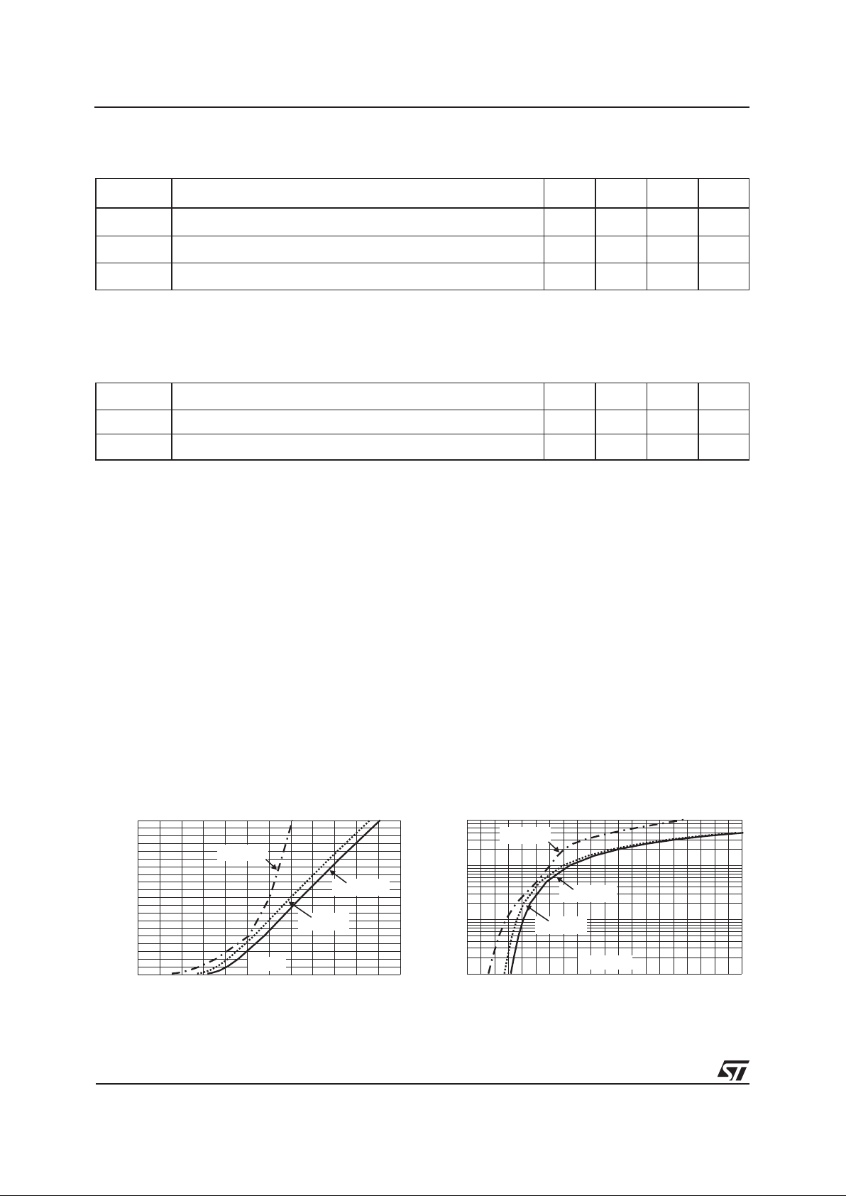
0.0 0.2 0.4 0.6 0.8 1.0 1.2
0.0E+0
2.0E-3
4.0E-3
6.0E-3
8.0E-3
1.0E-2
1.2E-2
1.4E-2
1.6E-2
1.8E-2
2.0E-2
VFM(V)
IFM(A)
Tj=100°C
Typical values
Tj=25°C
Maximum values
Tj=25°C
Typical values
Fig. 1-1: Forward voltage drop versus forward
current (low level).
0.0 0.2 0.4 0.6 0.8 1.0 1.2 1.4 1.6 1.8 2.0
1E-4
1E-3
1E-2
7E-2
VFM(V)
IFM(A)
Tj=100°C
Typical values
Tj=25°C
Maximum values
Tj=25°C
Typical values
Fig. 1-2: Forward voltage drop versus forward
current (high level).
* Effective carrier life time.
Pulse test: * tp = 380µs, δ < 2%
** tp = 5 ms, δ < 2%
Page 3

BAR 18 / BAS70-04 06
3/4
1 10 100
0.1
1.0
2.0
VR(V)
C(pF)
F=1MHz
Tj=25°C
Fig.4: Junctioncapacitance versus reversevoltage
applied (typical values).
1E-3 1E-2 1E-1 1E+0 1E+1 1E+2
0.01
0.10
1.00
tp(s)
Zth(j-a)/Rth(j-a)
T
δ
=tp/T
tp
Single pulse
δ = 0.1
δ = 0.2
δ = 0.5
Fig. 5: Relative variation of thermal impedance
junction to ambient versus pulse duration (alumine
substrate 10mm*8mm*0.5mm).
0 5 10 15 20 25 30 35 40 45 50
150
200
250
300
350
S(Cu) (mm²)
Rth(j-a) (°C/W)
P=0.25W
Fig. 6: Thermal resistance junction to ambient versuscopper surfaceunder each lead(Epoxy printed
circuit board FR4, copper thickness: 35µm).
0 5 10 15 20 25 30 35 40 45 50 55 60 65 70
1E-3
1E-2
1E-1
1E+0
1E+1
VR(V)
IR(µA)
Tj=25°C
Tj=100°C
Fig. 2: Reverse leakage current versus reverse
voltage applied (typical values).
0 25 50 75 100 125 150
1E-2
1E-1
1E+0
1E+1
1E+2
5E+2
Tj(°C)
IR(µA)
VR=70V
Fig. 3: Reverse leakage current versus junction
temperature (typical values)
Page 4

BAR 18 / BAS70-04 06
4/4
PACKAGE MECHANICAL DATA
SOT23 (Plastic)
B
E
S
e
e1
A
D
c
L
H
A1
0.9
0.035
0.9
0.035
1.9
0.075
mm
inch
2.35
0.92
1.1
0.043
1.1
0.043
1.45
0.037
0.9
0.035
FOOTPRINT DIMENSIONS
REF.
DIMENSIONS
Millimeters Inches
Min. Max. Min. Max.
A 0.89 1.4 0.035 0.055
A1 0 0.1 0 0.004
B 0.3 0.51 0.012 0.02
c 0.085 0.18 0.003 0.007
D 2.75 3.04 0.108 0.12
e 0.85 1.05 0.033 0.041
e1 1.7 2.1 0.067 0.083
E 1.2 1.6 0.047 0.063
H 2.1 2.75 0.083 0.108
L 0.6 typ. 0.024 typ.
S 0.35 0.65 0.014 0.026
Informationfurnished is believed to be accurate and reliable. However, STMicroelectronics assumes no responsibility for the consequences of
useof such information nor forany infringement of patents orother rights of third parties which may result from its use. No license is granted by
implication or otherwise under any patent or patent rights of STMicroelectronics. Specifications mentioned in this publication are subject to
change without notice. This publication supersedes and replaces all information previously supplied.
STMicroelectronics products are not authorized for use as critical components in life support devices or systems without express written
approval of STMicroelectronics.
The ST logo is a registered trademark of STMicroelectronics
© 2001 STMicroelectronics - Printed in Italy - All rights reserved.
STMicroelectronics GROUP OF COMPANIES
Australia - Brazil - Canada - China - Finland - France - Germany
Hong Kong - India - Israel - Italy - Japan - Malaysia - Malta - Morocco - Singapore
Spain - Sweden - Switzerland - United Kingdom - United States.
http://www.st.com
Ordering type Marking Package Weight Base qty Delivery mode
BAR18 D76 SOT-23 0.01g 3000 Tape & reel
BAS70-04 D96 SOT-23 0.01g 3000 Tape & reel
BAS70-05 D97 SOT-23 0.01g 3000 Tape & reel
BAS70-06 D98 SOT-23 0.01g 3000 Tape & reel
■
Epoxy meets UL94,V0
 Loading...