

Page 1
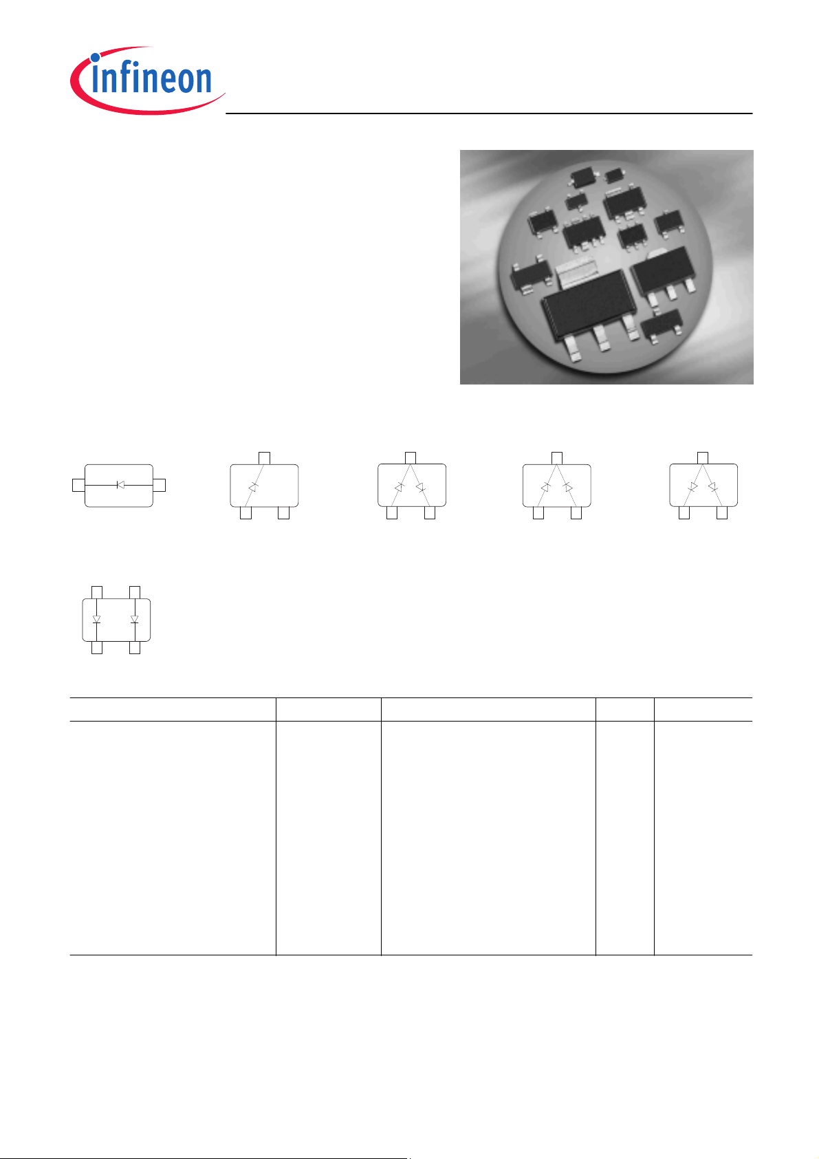
Silicon Schottky Diode
• General-purpose diode for high-speed switching
• Circuit protection
• Voltage clamping
• High-level detecting and mixing
BAS40.../BAS140W
BAS140W
BAS40-02L
1 2
BAS40 BAS40-04
3
1 2
3
D 1
D 2
1
2
BAS40-05
BAS40-05W
3
D 2
D 1
1
2
BAS40-07
BAS40-07W
34
D 2
D 1
1
2
ESD (Electrostatic discharge) sensitive device, observe handling precaution!
Type Package Configuration L
BAS140W
BAS40
BAS40-02L
BAS40-04
SOD323
SOT23
TSLP-2-1
SOT23
single
single
single, leadless
series
(nH) Marking
S
1.8
1.8
0.4
1.8
BAS40-06
BAS40-06W
3
D 2
D 1
1
2
white 4
43s
FF
44s
BAS40-05
BAS40-05W
BAS40-06
BAS40-06W
BAS40-07
BAS40-07W
SOT23
SOT323
SOT23
SOT323
SOT143
SOT343
common cathode
common cathode
common anode
common anode
parallel pair
parallel pair
1
1.8
1.4
1.8
1.4
2
1.6
45s
45s
46s
46s
47s
47s
2006-07-18
Page 2

Maximum Ratings at TA = 25°C, unless otherwise specified
BAS40.../BAS140W
Parameter
Symbol Value Unit
Diode reverse voltage V
Forward current I
Non-repetitive peak surge forward current
I
t ≤ 10ms
Total power dissipation
BAS140W, T
BAS40, BAS40-07, T
BAS40-02L, T
≤ 113°C
S
≤ 127°C
S
≤ 81°C
S
BAS40-04, BAS40-06, T
BAS40-06W, T
BAS40-05, T
BAS40-05W, T
BAS40-07W, T
≤ 106°C
S
≤ 31°C
S
≤ 98°C
S
≤ 118°C
S
≤ 56°C
S
P
Junction temperature T
R
F
FSM
tot
j
40 V
120 mA
200
mW
250
250
250
250
250
250
250
250
150 °C
Operating temperature range T
Storage temperature T
Thermal Resistance
Parameter
Junction - soldering point1)
BAS140W
BAS40, BAS40-07
BAS40-02L
BAS40-04, BAS40-06
BAS40-06W
BAS40-05
BAS40-05W
BAS40-07W
1
For calculation of R
please refer to Application Note Thermal Resistance
thJA
op
stg
-55 ... 125
-55 ... 150
Symbol Value Unit
R
thJS
K/W
≤ 150
≤ 275
≤ 90
≤ 375
≤ 175
≤ 475
≤ 205
≤ 125
2
2006-07-18
Page 3

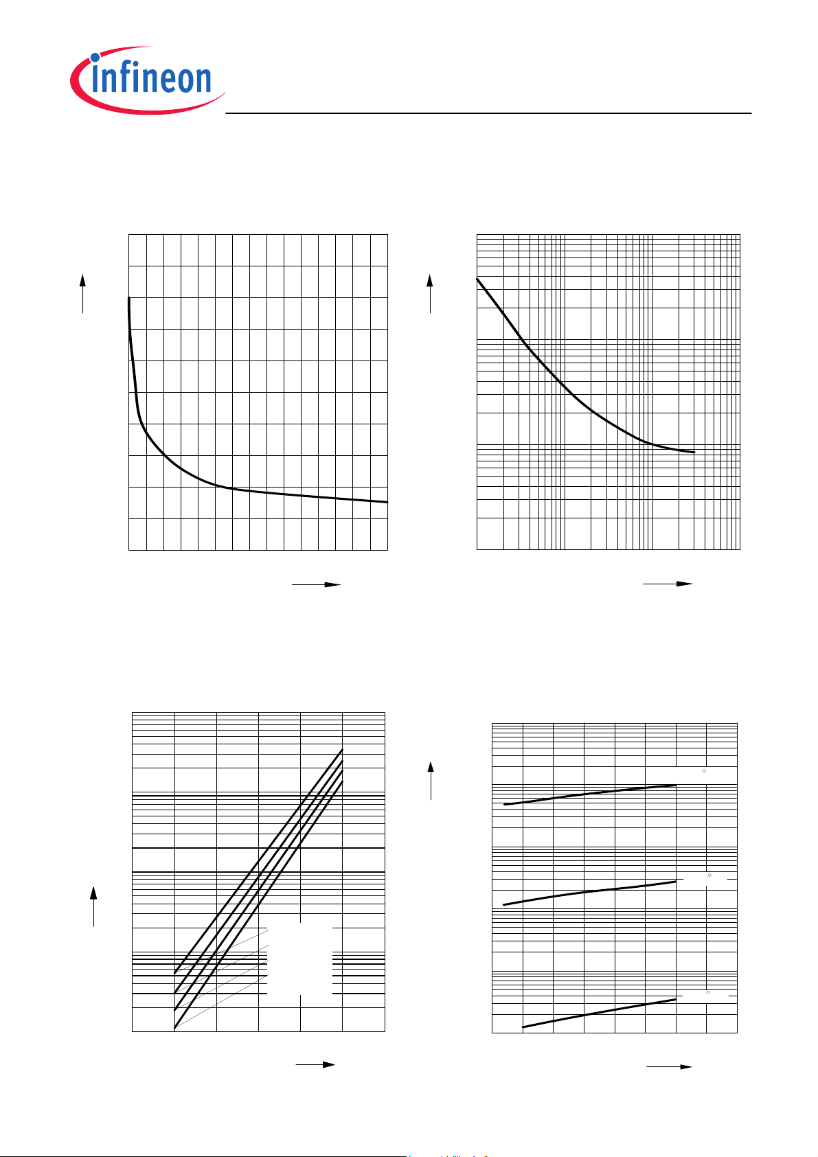
Electrical Characteristics at TA = 25°C, unless otherwise specified
BAS40.../BAS140W
Parameter
DC Characteristics
Breakdown voltage
I
= 10 µA
(BR)
Reverse current
V
= 30 V
R
Forward voltage
I
= 1 mA
F
I
= 10 mA
F
I
= 40 mA
F
Forward voltage matching1)
I
= 10 mA
F
AC Characteristics
Diode capacitance
V
= 0 , f = 1 MHz
R
Symbol Values Unit
min. typ. max.
V
(BR)
I
R
V
F
∆ V
C
T
F
40 - - V
- - 1
250
350
600
310
450
720
380
500
1000
- - 20
- 3 5 pF
µA
mV
Differential forward resistance
= 10 mA, f = 10 kHz
I
F
Charge carrier life time
I
= 25 mA
F
1
∆V
is the difference between lowest and highest VF in a multiple diode component.
F
R
τ
F
rr
- 10 - Ω
- - 100 ps
3
2006-07-18
Page 4
BAS40.../BAS140W
Diode capacitance C
f = 1MHz
5
C
T
pF
4
3
2
1
0
0
10 20 V 30
= ƒ (V
T
)
R
Forward resistance r
= ƒ (I
f
)
F
f = 10 kHz
EHB00040BAS 40...
V
R
3
10
r
f
Ω
2
10
1
10
3
10
0.1
1 10 mA 100
EHB00041BAS 40...
Ι
F
Reverse current I
= Parameter
V
R
-4
10
A
-5
10
R
I
-6
10
-7
10
-8
10
0 25 50 75 100
= ƒ (T
R
)
A
VR = 40V
30V
20V
10V
°C
Reverse current I
= Parameter
T
A
3
10
Ι
R
µ
A
2
10
1
10
= ƒ(V
R
)
R
EHB00039BAS 40...
TA= 150 C
85 C
0
10
-1
10
25 C
-2
150
T
A
10
0
10 20 30 V 40
V
R
4
2006-07-18
Page 5
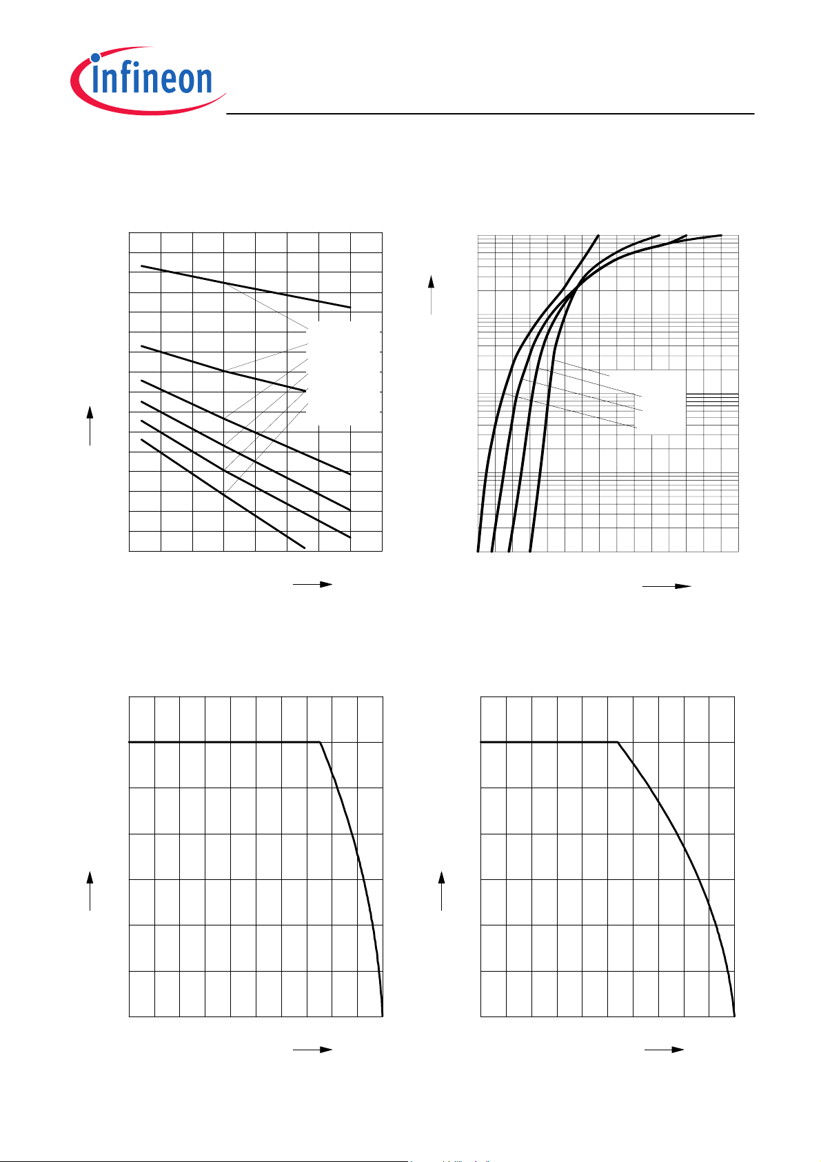
BAS40.../BAS140W
Forward Voltage V
= Parameter
I
F
0.8
V
0.6
F
0.5
V
0.4
0.3
0.2
0.1
0
-50 -25 0 25 50 75 100
= ƒ (T
F
)
A
IF = 40 mA
10 mA
1 mA
0.1 mA
10 µA
1 µA
°C
T
A
150
Forward current I
= Parameter
T
A
2
10
Ι
F
mA
1
10
0
10
-1
10
-2
10
0.0
= ƒ (V
F
)
F
T
A
EHB00038BAS 40...
= -40 ˚C
25 ˚C
85 ˚C
150 ˚C
0.5 1.0 V 1.5
V
F
Forward current I
BAS140W
140
mA
100
F
I
80
60
40
20
0
0 15 30 45 60 75 90 105 120
= ƒ (T
F
)
S
Forward current I
= ƒ (T
F
)
S
BAS40, BAS40-07
140
mA
100
F
I
80
60
40
20
0
0 15 30 45 60 75 90 105 120
°C
150
T
S
T
°C
150
S
5
2006-07-18
Page 6

BAS40.../BAS140W
Forward current I
BAS40-02L
140
mA
100
F
I
80
60
40
20
0
0 15 30 45 60 75 90 105 120
= ƒ (T
F
)
S
Forward current I
= ƒ (T
F
)
S
BAS40-04, BAS40-06
140
mA
100
F
I
80
60
40
20
0
0 15 30 45 60 75 90 105 120
°C
150
T
S
T
°C
150
S
Forward current I
BAS40-06W
140
mA
100
F
I
80
60
40
20
0
0 15 30 45 60 75 90 105 120
= ƒ (T
F
)
S
Forward current I
= ƒ (T
F
)
S
BAS40-05
140
mA
100
F
I
80
60
40
20
0
0 15 30 45 60 75 90 105 120
°C
150
T
S
T
°C
150
S
6
2006-07-18
Page 7

BAS40.../BAS140W
Forward current I
BAS40-05W
140
mA
100
F
I
80
60
40
20
0
0 15 30 45 60 75 90 105 120
= ƒ (T
F
)
S
Forward current I
= ƒ (T
F
)
S
BAS40-07W
140
mA
100
F
I
80
60
40
20
0
0 15 30 45 60 75 90 105 120
°C
150
T
S
T
°C
150
S
Permissible Puls Load R
BAS140W
BAS 140W
5
K/W
R
thJS
2
10
5
1
10
5
t
D =
T
0
10
10-610-510-410-310
p
thJS
= ƒ (t
D =
0.5
0.2
0.1
0.05
0.02
0.01
0.005
0
t
p
T
-2
)
p
EHD07165
s10
t
p
0
Permissible Pulse Load
I
Fmax
/ I
FDC
= ƒ (t
)
p
BAS140W
BAS 140W
2
10
Ι
F
max
Ι
DC
F
5
1
10
5
0
10
10-610-510-410-310
D =
t
p
T
D =
0
0.005
0.01
0.02
0.05
0.1
0.2
0.5
EHD07166
t
p
T
-2
s10
t
p
0
7
2006-07-18
Page 8

BAS40.../BAS140W
Permissible Puls Load R
BAS40-02L
2
10
K/W
thJS
R
10
0.5
0.2
0.1
0.05
0.02
0.01
0.005
D = 0
-4
-3
10
10
10
1
0
10
-6
-5
10
thJS
10
-2
= ƒ (t
-1
10
)
p
Permissible Pulse Load
I
Fmax
/ I
FDC
= ƒ (t
)
p
BAS40-02L
1
10
FDC
/I
10
D = 0
0.005
0.01
0.02
0.05
0.1
0.2
0.5
-4
10
-3
10
-2
s
t
0
10
p
Fmax
I
-
0
10
s
t
1
10
p
10
-6
10
-5
Permissible Puls Load R
BAS40-06W
3
10
K/W
2
10
thJS
R
0.5
10
-4
0.2
0.1
0.05
0.02
0.01
0.005
D = 0
10
10
10
1
0
10
-6
10
-5
thJS
-3
= ƒ (t
-2
10
)
p
Permissible Pulse Load
I
Fmax
/ I
FDC
= ƒ (t
)
p
BAS40-06W
2
10
-
FDC
/I
10
D = 0
0.005
0.01
0.02
0.05
0.1
0.2
0.5
-4
10
-3
10
-2
s
t
0
10
p
Fmax
I
1
10
0
10
s
t
0
10
p
10
-6
10
-5
8
2006-07-18
Page 9

BAS40.../BAS140W
Permissible Puls Load R
BAS40-05W
3
10
K/W
2
10
hJS
Rt
0.5
10
-4
0.2
0.1
0.05
0.02
0.01
0.005
D = 0
10
10
10
1
0
10
-6
10
-5
thJS
-3
= ƒ (t
-2
10
)
p
Permissible Pulse Load
I
Fmax
/ I
FDC
= ƒ (t
)
p
BAS40-05W
2
10
-
FDC
/I
10
D = 0
0.005
0.01
0.02
0.05
0.1
0.2
0.5
-4
10
-3
10
-2
s
t
0
10
p
Fmax
I
1
10
0
s
t
0
10
p
10
10
-6
10
-5
9
2006-07-18
Page 10

Package Outline
Foot Print
Package SOD323
+0.2
1.25
-0.1
2
1
0.3
+0.1
-0.05
M
A
Cathode
marking
±0.2
2.5
0.25
0
±0.05
±0.15
0.45
0.9
+0.2
-0.1
0.15
+0.2
0.3
+0.1
-0.06
BAS40.../BAS140W
A
-0.1
1.7
+0.05
-0.2
Marking Layout (Example)
Standard Packing
0.80.8
1.7
0.6
BAR63-03W
Type code
Cathode marking
Laser marking
Reel ø180 mm = 3.000 Pieces/Reel
Reel ø330 mm = 10.000 Pieces/Reel
Cathode
marking
4
8
2
2.9
0.65
0.2
1
1.35
10
2006-07-18
Page 11

Package Outline
Foot Print
Package SOT143
±0.1
0.8
0.2
+0.1
-0.05
2.9
1.9
12
1.7
B
34
+0.1
0.4
-0.05
0.8 0.81.2
0.25MB
0.15 MIN.
±0.15
2.4
0.2
BAS40.../BAS140W
±0.1
1
0.1 MAX.
±0.1
1.3
10˚ MAX.
0.08...0.15
0...8˚
M
A
10˚ MAX.
A
Marking Layout (Example)
Standard Packing
Reel ø180 mm = 3.000 Pieces/Reel
Reel ø330 mm = 10.000 Pieces/Reel
Pin 1
1.2
0.8
RF s
4
0.8
0.9 1.1 0.9
Manufacturer
2005, June
56
Date code (YM)
BFP181
Type code
0.2
Pin 1
3.15
11
8
2.6
1.15
2006-07-18
Page 12

Package Outline
Foot Print
Package SOT23
±0.1
2.9
12
1)
+0.1
0.4
-0.05
1.9
0.25MBC
1) Lead width can be 0.6 max. in dambar area
B
3
C
0.95
0.8
0.15 MIN.
±0.15
2.4
0.2
±0.1
1
0.1 MAX.
10˚ MAX.
0.08...0.15
0...8˚
M
A
BAS40.../BAS140W
±0.1
1.3
10˚ MAX.
A
Marking Layout (Example)
Standard Packing
Reel ø180 mm = 3.000 Pieces/Reel
Reel ø330 mm = 10.000 Pieces/Reel
Pin 1
0.8 1.2
EH
4
0.9
s
0.9 0.91.3
Manufacturer
2005, June
Date code (YM)
BCW66
Type code
0.2
Pin 1
3.15
2.13
12
2.65
8
1.15
2006-07-18
Page 13

Package Outline
Package SOT323
±0.2
2
0.3
+0.1
-0.05
3x
M
0.1
3
0.1 MAX.
0.1
0.9
BAS40.../BAS140W
±0.1
A
Foot Print
Marking Layout (Example)
12
0.650.65
0.6
0.8
0.65
0.65
1.6
±0.1
2.1
0.1 MIN.
M
0.2 A
0.15
+0.1
-0.05
±0.1
1.25
Standard Packing
Reel ø180 mm = 3.000 Pieces/Reel
Reel ø330 mm = 10.000 Pieces/Reel
Pin 1
Pin 1
2.15
Manufacturer
2005, June
Date code (YM)
BCR108W
Type code
4
8
2.3
0.2
1.1
13
2006-07-18
Page 14

Package Outline
Package TSLP-2-1
BAS40.../BAS140W
Top view Bottom view
0.05 MAX.
2
1
Cathode
marking
1) Dimension applies to plated terminal
0.4
+0.1
0.5
±0.05
0.65
±0.035
±0.05
0.6
2
1
1)
Foot Print
For board assembly information please refer to Infineon website "Packages"
0.6
1
Copper Solder mask Stencil apertures
0.35
0.3
0.35
0.45
0.275
0.925
0.375
0.275
1)
±0.035
0.25
±0.05
1
Marking Layout (Example)
Standard Packing
Reel ø180 mm = 15.000 Pieces/Reel
Reel ø330 mm = 50.000 Pieces/Reel (optional)
Cathode
marking
4
0.76
1.16
BAS16-02L
Type code
Cathode marking
Laser marking
0.5
8
14
2006-07-18
Page 15

BAS40.../BAS140W
Edition 2006-02-01
Published by
Infineon Technologies AG
81726 München, Germany
© Infineon Technologies AG 2006.
All Rights Reserved.
Attention please!
The information given in this dokument shall in no event be regarded as a guarantee
of conditions or characteristics (“Beschaffenheitsgarantie”). With respect to any
examples or hints given herein, any typical values stated herein and/or any information
regarding the application of the device, Infineon Technologies hereby disclaims any
and all warranties and liabilities of any kind, including without limitation warranties of
non-infringement of intellectual property rights of any third party.
Information
For further information on technology, delivery terms and conditions and prices
please contact your nearest Infineon Technologies Office (www.infineon.com).
Warnings
Due to technical requirements components may contain dangerous substances.
For information on the types in question please contact your nearest
Infineon Technologies Office.
Infineon Technologies Components may only be used in life-support devices or
systems with the express written approval of Infineon Technologies, if a failure of
such components can reasonably be expected to cause the failure of that
life-support device or system, or to affect the safety or effectiveness of that
device or system.
Life support devices or systems are intended to be implanted in the human body,
or to support and/or maintain and sustain and/or protect human life. If they fail,
it is reasonable to assume that the health of the user or other persons
may be endangered.
15
2006-07-18
 Loading...