Page 1

SOT23 SILICON HIGH
SPEED SWITCHING DIODE
ISSUE 2 JANUARY 1995
BAS19
BAS20
BAS21
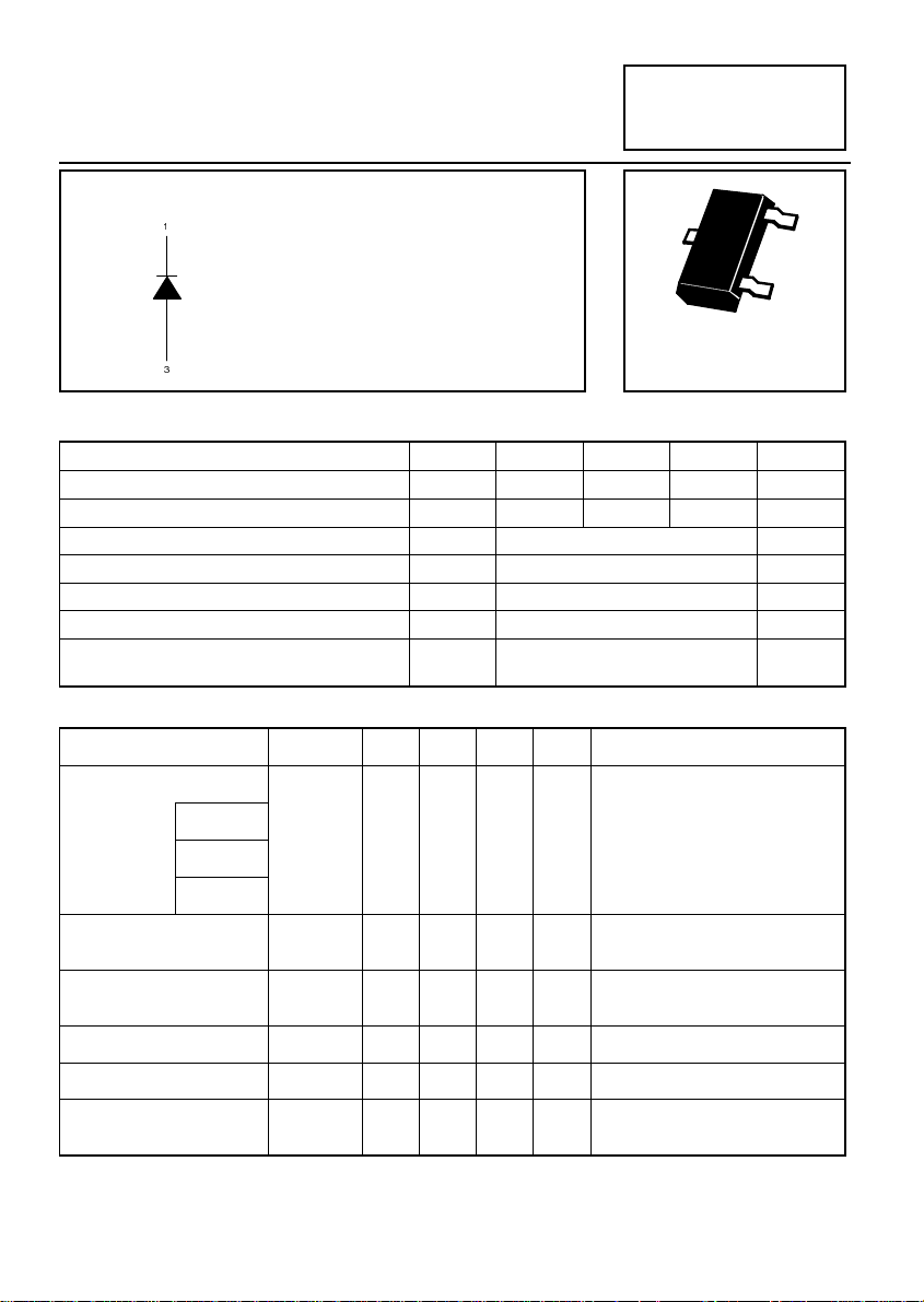
PIN CONFIGURATION
1
PARTMARKING DETAILS
1
3
BAS19 A8
BAS20 A81
3
BAS21 A82
SOT23
ABSOLUTE MAXIMUM RATINGS.
PARAMETER SYMBOL BAS19 BAS20 BAS21 UNIT
Continuous Reverse Voltage V
Repetative Peak Reverse Voltage V
Average Forward Rectified Current I
Forward Current I
Repetative Peak Forward Current I
Power Dissipation at T
=25°C P
amb
Operating and Storage Temperature
Range
ELECTRICAL CHARACTERISTICS (at T
R
RRM
F(AV)
F
FRM
tot
T
j:Tstg
= 25°C unless otherwise stated).
amb
PARAMETER SYMBOL MIN. TYP. MAX. UNIT CONDITIONS.
Reverse
Breakdown
Voltage
BAS19 120 V
V
(BR)
BAS20 200 V
BAS21 250 V
Reverse Current I
Static Forward Voltage V
Differential Resistance r
Diode Capacitance C
Reverse Recovery Time t
R
rr
diff
F
5
d
100 150 200 V
120 200 250 V
200 mA
200 mA
625 mA
330 mW
-55 to +150 °C
=100µA (1)
I
R
=100µA (1)
I
R
=100µA (2)
I
R
nA
µA
Ω
V
max
R=VR
max, TJ=150°C
V
R=VR
IF=100mA
=200mA
I
F
IF=10mA
100
100
1.00
1.25
5pFf=1MHz
50 ns IF=30mA to IR=30mA
=10Ω measured at I
R
L
=3mA
R
2
(1) Measured under pulsed conditions. Pulse width=300µs. Duty cycle ≤ 2%
(2) At zero life time, measured under pulse conditions to avoid excessive dissipation and voltage
limited to 275V
Spice parameter data is available upon request for this device
PAGE NO
Page 2

BAS19
BAS20
BAS21
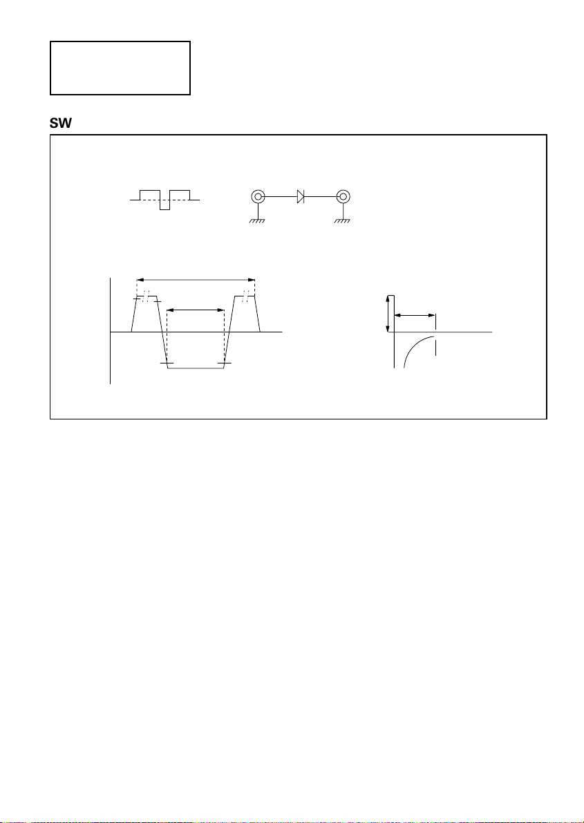
SWITCHING TIME TEST DATA
Recovery Time Equivalent Test Circuit
Pulse Generator
RS=50
Ω
t
V
90%
p(tot )
10%
t
90%
Input Signal Output Signal
Input Signal
Total Pulse Duration t
Duty Factor
Rise Time of Reverse
Pulse
p
DUT
Reverse Pulse Duration t
p(tot)
δ
t
r
2µs
0.0025
0.6ns
Oscilloscope
Rise Time t
Circuit Capacitance* C <1pF
Sampling Oscilloscope
+I
=50Ω
R
IN
t
rr
F
t
I
R*
100ns
p
0.35ns
r
 Loading...