Page 1

Product Catalog > Diodes > Switching Diodes >
Part Number BAS20
product family SMALL SIGNAL DIODES
package type SOT-23
VRM(PRV) 200V
Ifsm 0.5A
IF(AV) 200mA
@Vf 1.25V
@If 200mA
Trr 50nS
IR 100nA
@VR 200V
Package Qty Tape : 3K/Reel, 30k/Box, 120K/Ctn;
This product is listed under the following categories where you may find similar products:
Diodes
Switching Diodes
Page 2

p
@
)
j
inches
MCC
Micro Commercial Components
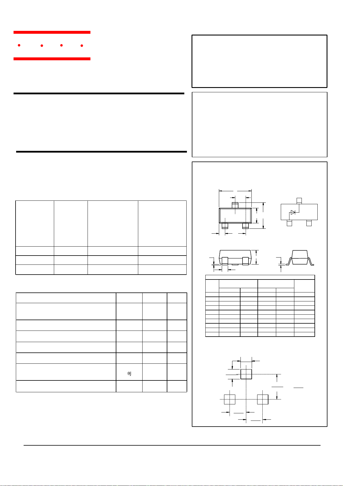
BAS19
TM
THRU
BAS21
Features
Ideally Suited for Automatic Insertion
150
o
C Junction Temperature
Fast Switching speed
Epitaxial Planar Die Construction
Mechanical Data
Case Material: Molded Plastic. UL Flammability
Classification Rating 94V-0 and MSL Rating 1
Weight: 0.008 grams ( approx.)
Continuous
MCC Part
Number
Marking
Reverse
Voltage
V (V)
R
BAS19 JP 100 120
BAS20 JR 150 200
BAS21 JS 200 250
Maximum Ratings @ 25oC Unless Otherwise Specified
Parameter Symbol Value Unit
Non-re
etitive Peak
Forward Surge Current @ t=1s
Average Rectified Forward Current
Forward DC Current at T
Repetitive Peak Forward Current
Power Dissipation up to T
Thermal Resistance Junction to
amb
amb
t=1us
=25oC
=25oC
I
FSM
I
F(AV
I
FRM
P
R
Ambient
T
Operating & Storage Temperature
,T
Repetitive
I
F
tot
q
JA
-65~150
STG
Peak
Reverse
Voltage
V (V)
RRM
2.5
0.5
(1)
200
(2)
200
625 mA
250 mW
430
A
mA
mA
o
C/W
o
C
Small
Signal Diodes
250mW
SOT-23
.079
2.000
Top View
1
mm
A
D
B
C
F
E
G
K
INCHES MM
DIM MIN MAX MIN MAX NOTE
A .110 .120 2.80 3.04
B .083 .098 2.10 2.64
C .047 .055 1.20 1.40
D .035 .041 .89 1.03
E .070 .081 1.78 2.05
F .018 .024 .45 .60
G .0005 .0039 .013 .100
H .035 .044 .89 1.12
J .003 .007 .085 .180
K .015 .020 .37 .51
Suggested Solder
.035
.900
H
DIMENSIONS
Pad Layout
.800
3
2
Notes: (1) Measured under pulse conditions;
Pulse time = t
(2) Device on fiberglass substrate,
See layout on next page
<= 0.3ms
p
1 of 3
.
.950
7
.037
.950
Page 3

BAS19 thru BAS21
MCC
Electrical Characteristics (T
= 25°C unless otherwise noted)
J
Parameter Symbol Test Condition Min Typ Max Unit
Forward Voltage V
Leakage Current I
Dynamic Forward Resistance r
Capacitance C
Reverse Recovery Time
(1)Device on fiberglass substrate, see layout (SOT-23).
(see figures) t
F
R
f
tot
rr
IF= 100mA — — 1.0 V
IF= 200mA — — 1.25 V
VR= V
VR= V
Rmax
; Tj= 150°C — — 100 µA
Rmax
— — 100 nA
IF= 10mA — 5 — Ω
VR= 0
f = 1MHz
IF= 30mA, I
R =
30mA
Irr= 3mA, RL= 100Ω
—— 5pF
— — 50 ns
Test Circuit and Waveforms(BAS19, BAS20, BAS21)
Micro Commercial Components
TM
Ω
Test circuit
Input Signal - total pulse duration tp(tot) = 2µs
- duty factor δ = 0.0025
- rise time of reverse pulse t
= 0.6ns
r
- reverse pulse duration tp= 100ns
Oscilloscope - rise time t
= 0.35ns
r
- cicuit capitance* C < 1pF
*C = oscilloscope input capactitance + parasitic capacitance
Layout for R
ΘJA
test
Thickness: Fiberglass 0.059 in. (1.5 mm)
Copper leads 0.012 in. (0.3 mm)
0.59 (15)
0.03 (0.8 )
0.47 (12)
0.30 (7.5 )
0.12 (3)
.04 (1)
.08 (2)
.04 (1)
.08 (2)
Input signal
Waveforms; IR = 3 mA
Output signal
0.2 (5)
2 of 3
0.06 (1.5)
Dimensions in inches (millimeters)
0.20 (5.1)
Page 4

MCC
Micro Commercial Components
Ordering Information
Device Packing
(Part Number)-TP Tape&Reel;3Kpcs/Reel
TM
***IMPORTANT NOTICE***
Micro Commercial Components Corp
product herein to make corrections, modifications , enhancements , improvements , or other changes .
Micro Commercial Components Corp
use of any product described herein; neither does it convey any license under its patent rights ,nor
the rights of others . The user of products in such applications shall assume all risks of such use
and will agree to hold Micro Commercial Components Corp
products are represented on our website, harmless against all damages.
***APPLICATIONS DISCLAIMER***
Products offer by Micro Commercial Components Corp
. reserves the right to make changes without further notice to any
. does not assume any liability arising out of the application or
. and all the companies whose
. are not intended for use in Medical,
Aerospace or Military Applications.
3 of 3
 Loading...