

Page 1
BAS 16W
Silicon Switching Diode
• For high speed switching applications
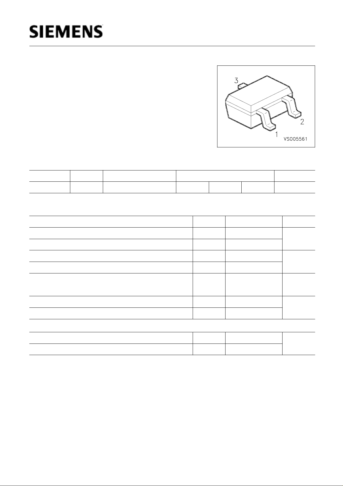
Type Marking Ordering Code Pin Configuration Package
BAS 16W A6s Q62702-A1050 1 = A 3 = C SOT-323
Maximum Ratings
Parameter Symbol Values Unit
Diode reverse voltage
Peak reverse voltage
Forward current
Surge forward current, t = 1 µs
Total Power dissipation
T
≤ 119 °C
S
Junction temperature
Storage temperature
V
V
I
I
P
T
T
R
RM
F
FS
tot
j
stg
75 V
85
250 mA
4.5
mW
250
150 °C
- 65 ... + 150
Thermal Resistance
Junction ambient
Junction - soldering point
1) Package mounted on epoxy pcb 40mm x 40mmm x 1.5mm / 0.5cm2 Cu
1)
R
R
thJA
thJS
≤
260 K/W
≤
125
Semiconductor Group 1 Nov-28-1996
Page 2

BAS 16W
Electrical Characteristics at
T
=25°C, unless otherwise specified
A
Parameter Symbol Values Unit
min. typ. max.
DC characteristics
Breakdown voltage
I
= 100 µA
(BR)
Forward voltage
I
= 1 mA
F
I
= 10 mA
F
I
= 50 mA
F
I
= 150 mA
F
Reverse current
V
= 70 V,
R
V
= 25 V,
R
V
= 75 V,
R
T
= 25 °C
A
T
= 150 °C
A
T
= 150 °C
A
V
V
I
R
(BR)
F
75 - -
-
-
-
-
-
-
-
-
-
-
-
-
-
-
V
mV
715
855
1000
1250
µA
1
30
50
AC characteristics
Diode capacitance
V
= 0 V, f = 20 MHz
R
Reverse recovery time
I
= 10 mA,
F
t
measured at 1 mA
rr
I
= 10 mA,
R
R
= 100
L
Ω
C
t
D
pF
- - 2
rr
ns
- - 6
Semiconductor Group 2 Nov-28-1996
Page 3

BAS 16W
Forward current
I
F
= f (
T
*;
A
* Package mounted on epoxy
300
mA
I
F
200
150
100
50
T
)
S
T
T
S
A
Forward current
T
= 25°C
A
I
F
= f (
V
)
F
0
0 20 40 60 80 100 120 °C 150
Permissible Pulse Load
3
10
K/W
R
thJS
2
10
1
10
R
thJS
0.5
0.2
0.1
0.05
0.02
0.01
0.005
D = 0
= f(
TA,T
S
t
)
p
Permissible Pulse Load
I
Fmax
/
I
FDC
= f(
t
)
p
2
10
I
/
I
FDC
10
-
D = 0
0.005
0.01
0.02
1
0.05
0.1
0.2
0.5
Fmax
10
0
10
-6
10
-5
10
-4
10
-3
10
-2
10
-1
t
p
0
10
s
10
0
10
-6
10
-5
10
-4
10
-3
10
-2
-1
10
10 0 s
t
p
Semiconductor Group 3 Nov-28-1996
Page 4

BAS 16W
Forward voltage
V
= f (
F
T
) Reverse current
A
I
= f (
R
T
)
A
Semiconductor Group
4 Nov-28-1996
 Loading...