

Page 1
DISCRETE SEMICONDUCTORS
DATA SH EET
ook, halfpage
M3D050
BAS15
High-speed diode
Product specification
Supersedes data of April 1996
File under Discrete Semiconductors, SC01
1996 Sep 10
Page 2
Philips Semiconductors Product specification
High-speed diode BAS15
FEATURES
• Hermetically sealed leaded glass
SOD68 (DO-34) package
• High switching speed: max. 4 ns
DESCRIPTION
The BAS15 is a high-speed switching diode fabricated in planar technology,
and encapsulated in the hermetically sealed leaded glass SOD68 (DO-34)
package.
• Continuous reverse voltage:
max. 50 V
• Repetitive peak reverse voltage:
max. 50 V
• Repetitive peak forward current:
max. 225 mA.
APPLICATIONS
• High-speed switching
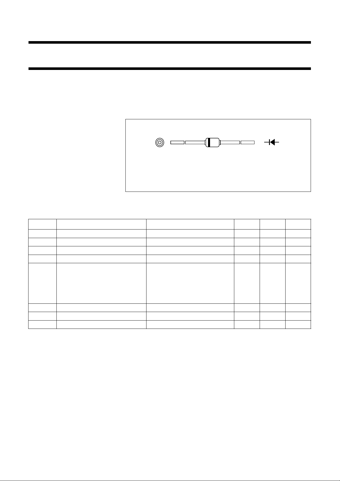
handbook, halfpage
The diode is type branded.
Fig.1 Simplified outline (SOD68; DO-34) and symbol.
k
a
MAM156
• Protection diodes in reed relays.
LIMITING VALUES
In accordance with the Absolute Maximum Rating System (IEC 134).
SYMBOL PARAMETER CONDITIONS MIN. MAX. UNIT
V
V
I
F
I
FRM
I
FSM
RRM
R
repetitive peak reverse voltage − 50 V
continuous reverse voltage − 50 V
continuous forward current see Fig.2; note 1 − 100 mA
repetitive peak forward current − 225 mA
non-repetitive peak forward current square wave; Tj=25°C prior to
surge; see Fig.4
t=1µs − 4A
t=1ms − 1A
t=1s − 0.5 A
P
tot
T
stg
T
j
total power dissipation T
storage temperature −65 +200 °C
junction temperature − 200 °C
=25°C; note 1 − 350 mW
amb
Note
1. Device mounted on an FR4 printed circuit-board; lead length 10 mm.
1996 Sep 10 2
Page 3

Philips Semiconductors Product specification
High-speed diode BAS15
ELECTRICAL CHARACTERISTICS
T
=25°C; unless otherwise specified.
j
SYMBOL PARAMETER CONDITIONS MIN. MAX. UNIT
V
F
I
R
C
d
t
rr
V
fr
forward voltage see Fig.3
=1mA − 700 mV
I
F
=10mA − 850 mV
I
F
= 100 mA − 1.1 V
I
F
reverse current see Fig.5
=30V − 50 nA
V
R
=50V − 200 nA
V
R
=30V; Tj= 150 °C − 75 µA
V
R
=50V; Tj= 150 °C − 100 µA
V
R
diode capacitance f = 1 MHz; VR= 0; see Fig.6 − 2pF
reverse recovery time when switched from IF= 10 mA to
− 4ns
IR= 60 mA; RL= 100 Ω;
measured at IR= 1 mA; see Fig.7
forward recovery voltage when switched from IF= 50 mA;
− 2.5 V
tr= 20 ns; see Fig.8
THERMAL CHARACTERISTICS
SYMBOL PARAMETER CONDITIONS VALUE UNIT
R
R
th j-tp
th j-a
thermal resistance from junction to tie-point lead length 10 mm 240 K/W
thermal resistance from junction to ambient lead length 10 mm; note 1 500 K/W
Note
1. Device mounted on a printed circuit-board without metallization pad.
1996 Sep 10 3
Page 4

Philips Semiconductors Product specification
High-speed diode BAS15
GRAPHICAL DATA
amb
MBG453
(oC)
200
handbook, halfpage
I
F
(mA)
100
0
0 100 200
Device mounted on a FR4 printed-circuit board; lead length 10mm.
T
Fig.2 Maximum permissible continuous forward
current as a function of ambient temperature.
300
handbook, halfpage
I
F
(mA)
200
100
0
012
(1) Tj= 175 °C; typical values.
(2) Tj=25°C; typical values.
(3) Tj=25°C; maximum values.
(1) (2) (3)
Fig.3 Forward current as a function of
forward voltage.
MBG465
VF (V)
2
10
handbook, full pagewidth
I
FSM
(A)
10
1
−1
10
1
Based on square wave currents.
Tj=25°C prior to surge.
Fig.4 Maximum permissible non-repetitive peak forward current as a function of pulse duration.
MBG704
10
2
10
3
10
tp (µs)
4
10
1996 Sep 10 4
Page 5

Philips Semiconductors Product specification
High-speed diode BAS15
3
10
handbook, halfpage
IR
(µA)
2
10
10
1
−1
10
−2
10
0 100
VR= 50 V.
Solid line; maximum values.
Dotted line; typical values.
Fig.5 Reverse current as a function of
junction temperature.
Tj (
MGD008
o
C)
200
1.2
handbook, halfpage
Cd
(pF)
1.0
0.8
0.6
0.4
01020
f = 1 MHz; Tj=25°C.
MGD004
VR (V)
Fig.6 Diode capacitance as a function of reverse
voltage; typical values.
1996 Sep 10 5
Page 6

Philips Semiconductors Product specification
High-speed diode BAS15
handbook, full pagewidth
R = 50SΩ
V = V I x R
RF S
(1) IR= 1 mA.
I
F
D.U.T.
SAMPLING
OSCILLOSCOPE
R = 50iΩ
MGA881
t
r
10%
V
R
90%
t
p
input signal
Fig.7 Reverse recovery voltage test circuit and waveforms.
t
I
F
t
rr
t
(1)
output signal
I
R = 50SΩ
Ω1 k Ω450
D.U.T.
I
OSCILLOSCOPE
R = 50iΩ
MGA882
Fig.8 Forward recovery voltage test circuit and waveforms.
1996 Sep 10 6
10%
t
r
90%
t
p
input
signal
V
V
fr
t
t
output
signal
Page 7

Philips Semiconductors Product specification
High-speed diode BAS15
PACKAGE OUTLINE
handbook, full pagewidth
Dimensions in mm.
1.6
max
25.4 min 25.4 min
3.04
max
0.55
max
MSA212 - 1
Fig.9 SOD68 (DO-34).
DEFINITIONS
Data Sheet Status
Objective specification This data sheet contains target or goal specifications for product development.
Preliminary specification This data sheet contains preliminary data; supplementary data may be published later.
Product specification This data sheet contains final product specifications.
Limiting values
Limiting values given are in accordance with the Absolute Maximum Rating System (IEC 134). Stress above one or
more of the limiting values may cause permanent damage to the device. These are stress ratings only and operation
of the device at these or at any other conditions above those given in the Characteristics sections of the specification
is not implied. Exposure to limiting values for extended periods may affect device reliability.
Application information
Where application information is given, it is advisory and does not form part of the specification.
LIFE SUPPORT APPLICATIONS
These products are not designed for use in life support appliances, devices, or systems where malfunction of these
products can reasonably be expected to result in personal injury. Philips customers using or selling these products for
use in such applications do so at their own risk and agree to fully indemnify Philips for any damages resulting from such
improper use or sale.
1996 Sep 10 7
 Loading...