

Page 1
Silicon RF Switching Diode
ll
Design for use in shunt configuration
l
Hight shunt signal isolation
l
Low shunt insertion loss
BAR 80
Type Marking Ordering code
(tape and reel)
BAR 80 AAs Q62702-A1084 C A C A MW-4
Maximum ratings
Parameter Symbol BAR 80 Unit
Reverse voltage
Forward current
Operating temperature range
Storage temperature range
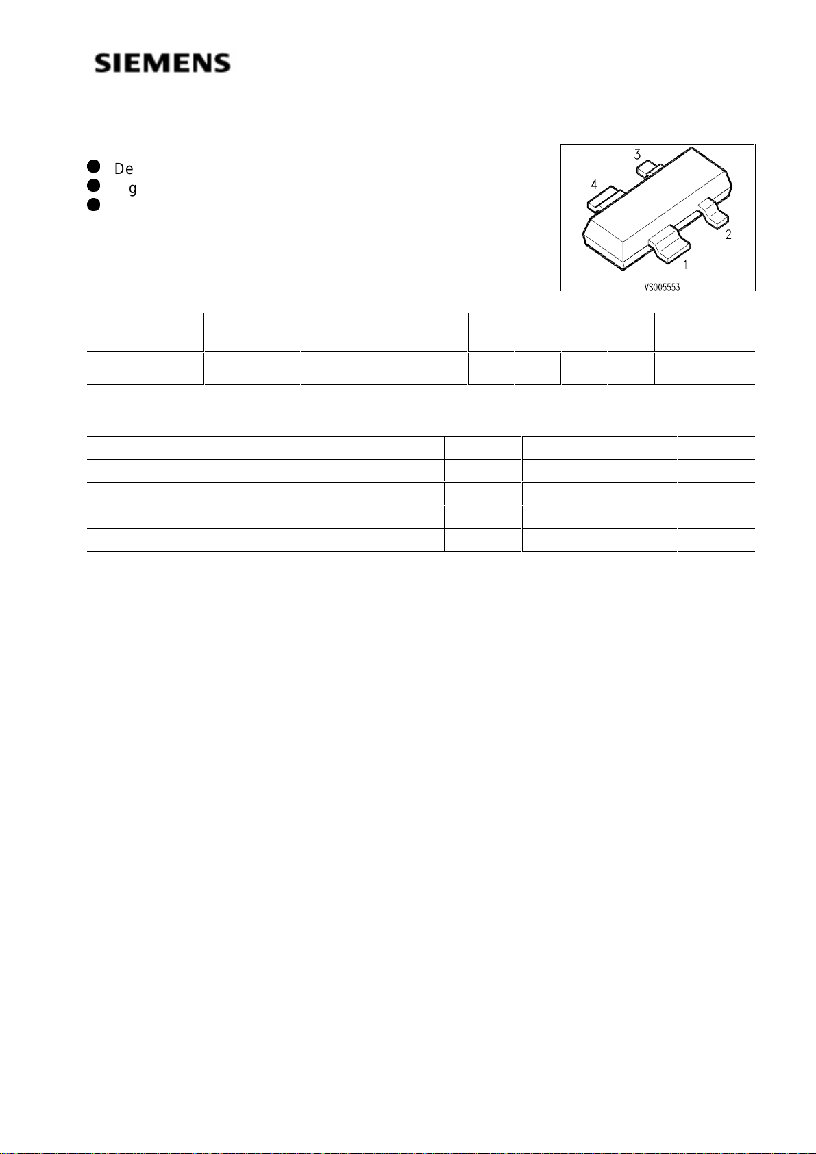
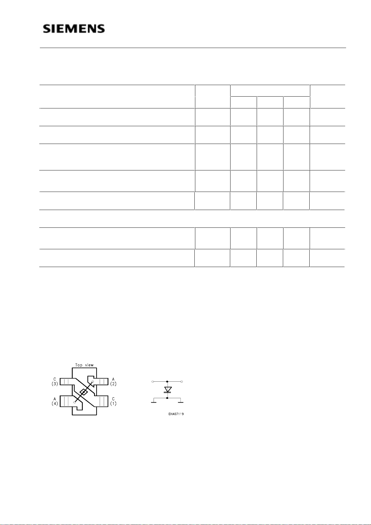
Pin configuration
1 2 3 4
V
R 35 V
I
F 100 mA
T
op -55...+125 °C
T
stg
-55...+150 °C
Package
1)
1) Package mounted on alumina 15mm x 16.7mm x 0.7mm
Semiconductor Group 1 Edition A02, 27.02.95
Page 2
BAR 80
Electrical characteristics
at
T
= 25 °C, unless otherwise specified.
A
Parameter Symbol Value Unit
min. typ. max.
Reverse current
V
R = 20 V
Forward voltage
I
F = 100 mA
Diode capacitance
V
R = 1 V,
V
R = 3 V,
f
= 1 MHz
f
= 1 MHz
Forward resistance f = 100MHz
I
F = 5 mA
I
V
C
r
R
--20
F
- 0.92 1
T
-
0.6
f
1
0.92
1.6
1.3
- 0.5 0.7
nA
V
pF
Ω
Series inductance to ground
Application information
Shunt signal isolation
I
F = 10 mA,
f
= 2 GHz,
R
=
R
G
Shunt insertion loss
V
R = 5 V,
f
= 2 GHz,
R
=
R
G
= 50 Ω
L
Configuration of the shunt-diode
= 50 Ω
L
L
s
nH
- 0.14 -
-
dB
-23-
I
L
dB
- 0.15 -
-A perfect ground is essential
for optimum isolation
-The anode pins should be used
as passage for RF
Semiconductor Group 2 Edition A02, 27.02.95
Page 3

BAR 80
Forward current
mA
I
F
I
F
= f (
TS,T
) Forward resistance
A
f
= 100 MHz
T
S
T
A
r
= (
f
I
)
F
Dioden capacitance
f
= 1 MHz
C
= f (
T
T
T
S
A
V
)
R
Semiconductor Group 3 Edition A02, 27.02.95
Page 4

BAR 80
Permissible pulse load
K/W
R
thJS
R
thJS
= f (
t
) Permissible pulse load
p
I
max
F
_______
I
DC
F
I
Fmax
/
I
FDC
= f (
t
)
p
t
p
t
p
Semiconductor Group 4 Edition A02, 27.02.95
 Loading...