

Page 1
BAR42FILM
®
SMALL SIGNAL SCHOTTKY DIODE
Table 1: Main Product Characteristics
I
F(AV)
V
RRM
T
j
(max) 0.33 and 0.40 V
V
F
FEATURES AND BENEFITS
■ Very small conduction losses
■ Negligible switching losses
■ Low forward voltage drop
■ Surface mount device
DESCRIPTION
Genral purpose metal to silicon diodes featuring
very low turn-on voltage and fast switching.
0.1 A
30 V
150°C
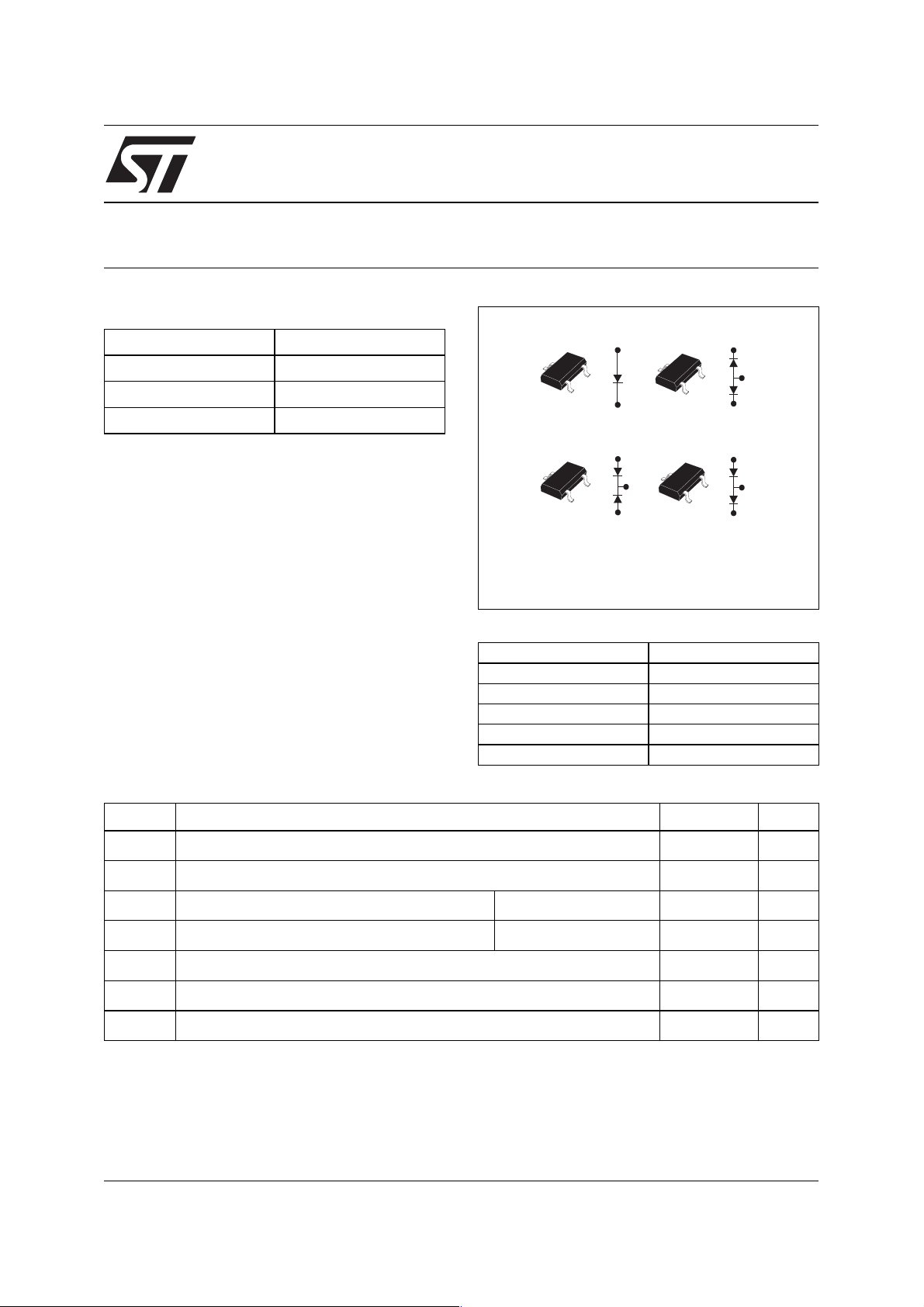
BAR43FILM
K
A
BAR42FILM
BAR43FILM
K
A1
BAR43CFILM
Table 2: Order Codes
Part Number Marking
BAR42FILM D94
BAR43FILM D95
BAR43AFILM DB1
BAR43CFILM DB2
BAR43SFILM DA5
A
Nc
K
A1
A2
K
A2
SOT23-3L
A
BAR43AFILM
A1
K2
BAR43ASFILM
K1
A
K1
K2
A2
K2
A2
A1
K1
K2
K1
Table 3: Absolute Ratings (limiting values)
Symbol Parameter Value Unit
V
RRM
I
F(AV)
I
FSM
P
T
T
T
Note 1: for double diodes, P
dPtot
------------- --
* : thermal runaway condition for a diode on its own heatsink
dTj
April 2005
Repetitive peak reverse voltage 30 V
Continuous forward current 0.1 A
Surge non repetitive forward current tp = 10ms sinusoidal 0.75 A
Power dissipation (note 1) T
tot
Maximum storage temperature range -65 to + 150 °C
stg
Maximum operating junction temperature * 150 °C
j
Maximum temperature for soldering during 10s 260 °C
L
is the total dissipation of both diodes.
tot
1
--------------- ----------->
Rth j a
–()
REV. 3
= 25°C 250 mW
amb
1/5
Page 2
BAR42FILM / BAR43FILM
Table 4: Thermal Resistance
Symbol Parameter Value Unit
R
th(j-a)
(*) Mounted on epoxy board with recommended pad layout.
Junction to ambient (*) 500 °C/W
Table 5: Static Electrical Characteristics
Symbol Parameter Tests conditions Min. Typ Max. Unit
V
I
R
V
F
Pulse test: * tp = 5 ms, δ < 2%
Breakdown voltage Tj = 25°C IR = 100µA 30 V
BR
T
= 25°C
*
Reverse leakage current
**
Forward voltage drop
** tp = 380 µs, δ < 2%
j
T
= 100°C
j
Tj = 25°C
BAR42
BAR43
ALL
= V
V
R
I
= 10mA
F
= 50mA
I
F
I
= 2mA
F
I
= 15mA
F
I
= 100mA
F
RRM
0.35 0.40
0.50 0.65
0.26 0.33
500 nA
100
0.45
1
Table 6: Dynamic Characteristics (Tj = 25°C)
Symbol Parameter Tests conditions Min. Typ. Max. Unit
µA
V
= 25°C VR = 1V F = 1 MHz
C Junction capacitance
t
Reverse recovery time
rr
η Detection efficiency
T
j
= 10 mA IR = 10 mA
I
F
T
= 25°C Irr = 1 mA RL = 100 Ω
j
C
= 300 pF F = 45 MHz
L
T
= 25°C Vi = 2 V RL = 50 Ω
j
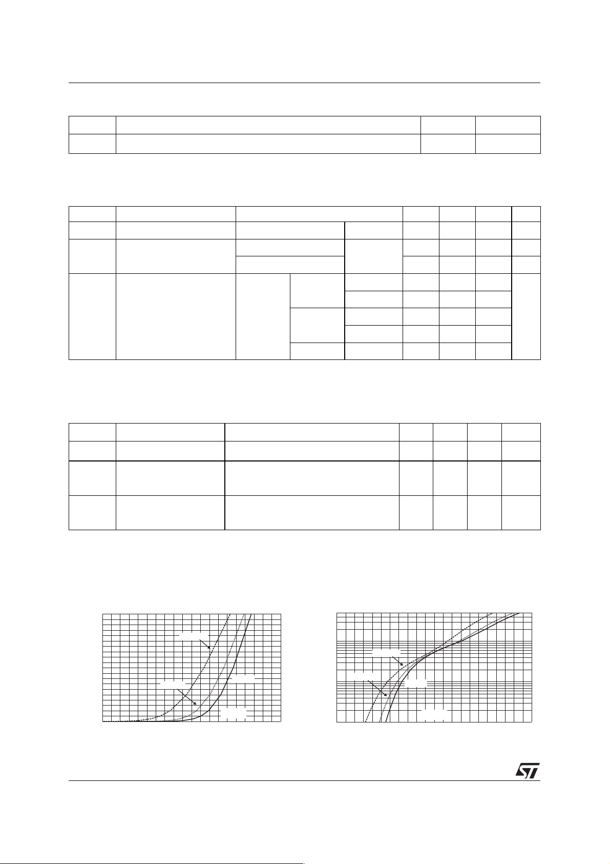
Figure 1: Forward voltage drop versus forward
current (typical values, low level)
I (A)
FM
2.00E-2
1.80E-2
1.60E-2
1.40E-2
1.20E-2
1.00E-2
8.00E-3
6.00E-3
4.00E-3
2.00E-3
0.00E+0
0.00 0.05 0.10 0.15 0.20 0.25 0.30 0.35 0.40 0.45 0.50
T =50°C
j
T =100°C
j
T =25°C
V (V)
FM
j
7pF
5ns
80 %
Figure 2: Forward voltage drop versus forward
current (typical values, high level)
I (A)
FM
5E-1
1E-1
T =100°C
j
T =50°C
1E-2
1E-3
j
0.0 0.1 0.2 0.3 0.4 0.5 0.6 0.7 0.8 0.9 1.0 1.1
T =25°C
j
V (V)
FM
2/5
Page 3

BAR42FILM / BAR43FILM
Figure 3: Reverse leakage current versus
reverse voltage applied (typical values)
I (µA)
R
1E+2
T =100°C
j
1E+1
1E+0
1E-1
1E-2
0 5 10 15 20 25 30
T =50°C
j
T =25°C
j
V (V)
R
Figure 5: Junction capacitance versus reverse
voltage applied (typical values)
C(pF)
10
5
F=1MHz
T =25°C
j
Figure 4: Reverse leakage current versus
junction temperature
I (µA)
R
1E+4
V =30V
1E+3
1E+2
1E+1
1E+0
1E-1
1E-2
R
V (V)
R
0 25 50 75 100 125 150
Figure 6: Relative variation of thermal
impedance junction to ambient versus pulse
duration (epoxy FR4 with recommended pad
layout, e(Cu)=35µm)
Z/R
th(j-a) th(j-a)
1.00
δ = 0.5
δ = 0.2
δ = 0.1
0.10
2
V (V)
1
12 5102030
R
Figure 7: Thermal resistance junction to
ambient versus copper surface under each
lead (Epoxy printed circuit board FR4, copper
thickness: 35µm)
R (°C/W)
th(j-a)
350
P=0.25W
300
250
200
150
0 5 10 15 20 25 30 35 40 45 50
S(CU)(mm²)
Single pulse
0.01
1E-3 1E-2 1E-1 1E+0 1E+1 1E+2
t (s)
p
δ
=tp/T
T
tp
3/5
Page 4

BAR42FILM / BAR43FILM
Figure 8: SOT23-3L Package Mechanical Data
A
E
e
B
L
H
e1
S
A1
c
D
Figure 9: Foot Print Dimensions (in millimeters)
0.95 0.61
DIMENSIONS
REF.
Millimeters Inches
Min. Max. Min. Max.
A 0.89 1.4 0.035 0.055
A1 0 0.1 0 0.004
B 0.3 0.51 0.012 0.02
c 0.085 0.18 0.003 0.007
D 2.75 3.04 0.108 0.12
e 0.85 1.05 0.033 0.041
e1 1.7 2.1 0.067 0.083
E 1.2 1.6 0.047 0.063
H 2.1 2.75 0.083 0.108
L 0.6 typ. 0.024 typ.
S 0.35 0.65 0.014 0.026
1.26
0.73
3.25
Table 7: Ordering Information
Ordering type Marking Package Weight Base qty Delivery mode
BAR42FILM D94
BAR43FILM D95
BAR43AFILM DB1
SOT23-3L 0.01 g 3000 Tape & reel
BAR43CFILM DB2
BAR43SFILM DA5
■ Epoxy meets UL94, V0
Table 8: Revision History
Date Revision Description of Changes
Aug-2001 2B Last update.
16-Apr-2005 3 Layout update. No content change.
4/5
Page 5

BAR42FILM / BAR43FILM
Information furnished is believed to be accurate and reliable. However, STMicroelectronics assumes no responsibility for the consequences
of use of such information nor for any infringement of patents or other rights of third parties which may result from its use. No license is granted
by implication or otherwise under any patent or patent rights of STMicroelectronics. Specifications mentioned in this publication are subject
to change without notice. This publication supersedes and replaces all information previously supplied. STMicroelectronics products are not
authorized for use as critical components in life support devices or systems without express written approval of STMicroelectronics.
The ST logo is a registered trademark of STMicroelectronics.
All other names are the property of their respective owners
© 2005 STMicroelectronics - All rights reserved
Australia - Belgium - Brazil - Canada - China - Czech Republic - Finland - France - Germany - Hong Kong - India - Israel - Italy - Japan -
Malaysia - Malta - Morocco - Singapore - Spain - Sweden - Switzerland - United Kingdom - United States of America
STMicroelectronics group of companies
www.st.com
5/5
Page 6

 Loading...