

Page 1

1
Multimedia ICs
High voltage controller for CRT
displays
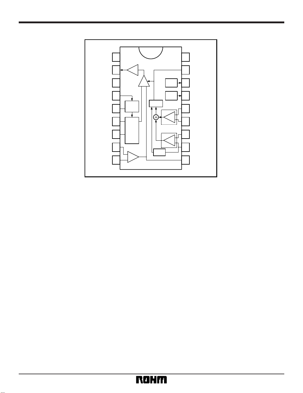
BA9755S
The BA9755S is an LSI chip with a chopper voltage controller designed to control the anode voltage of multiscan
monitors and other CRTs. There are two internal high-precision power supplies, each with an output voltage precision of ±1%. Using a high-precision voltage detection resistor makes it possible to set anode voltage without adjustment. Other internal components include an output voltage error detector and an overcurrent detector, which detects
overcurrent when the power is turned on.
•
Applications
CRT displays and HDTV products
•
Features
1) Internal chopper voltage controller.
2) Two internal high-precision power supplies, each
with an output voltage precision of ±1%.
3) Internal output voltage error detector.
4) Internal buffer circuit that directly drives power MOSFET for output drive.
•
Absolute maximum ratings (Ta = 25°C)
•
Recommended operating voltage (Ta = 25°C)
Parameter Symbol Limits Unit
Applied voltage 1
V
CC118
∗
1
V
Applied voltage 2
V
CC220
∗
2
V
Power dissipation
Pd 600
∗
1
mW
Operating temperature
Topr – 25 ~ + 75 °C
Storage temperature
Tstg – 55 ~ + 125 °C
∗
3 Reduced by 6.0mW for each increase in Ta of 1°C over 25°C.
∗
1 18pin ∗ 2 3pin
Parameter Symbol Limits Unit
Applied voltage 1 V
CC111 ~ 13 V
Applied voltage 2 V
CC211 ~ 16 V
∗
Used with condition
V
CC2 ⭌ VCC1
Page 2
2
Multimedia ICs BA9755S
•
Block diagram
1
2
3
4
5
6
7
8
9
18
17
16
15
14
13
12
11
10
PROTOUT
VREG9
VREG6
XREF
XRAYIN
ABLIN
PONDET
ERROUT
GND
PWMOUT
HDIN
MMCR
SAWOUT
AGC
ERRIN
ERRREF
+
–
SAW
GEN.
AGC
TYPE
+
–
REF
9.0V
REF
6.0V
+
–
LATCH
+
–
GND
Buffer
START
M. M.
PV
CC
Power VCC
VCC
Sig VCC
Page 3

3
Multimedia ICs BA9755S
Pin No.
Pin name
1
GND
Ground
This is the common ground for the small signal system and the power system, and so requires
a stable ground suitable for common impedance.
2
PWMOUT
PWM wave output
Output is fixed at the low level when the protector circuit or thermal shutdown circuit is activated.
3
PV
CC
Power supply for the power system. Place a decoupling capacitor in proximity to this pin.
4
HDIN
HD pulse input. The input signal should be shorter than the rise time (
µs).
5
MMCR
Shifts the phase of the serrated wave. Use a charge resistance higher than 4.7kΩ.
Internal mono-multi time constant setting.
6
SAWOUT
f
Max. 80kHz→C = 1500p, fMax. 60kHz→C = 2000p
7
AGC
Set capacity according to the linearity of the minimum oscillation frequency and the response
time during frequency change.
AGC time constant setting.
8
ERRIN
Input of the error amplifiers feedback voltage.
9
ERRREF
Input of the error amplifiers feedback voltage.
When this voltage is given a time constant, the IC soft-starts when the power is turned on.
10
ERROUT
Output of the error detection voltage.
11
PON DET
12
ABLIN
Beam protector input. When the protector is activated, the latch locks and PWM output is fixed
at the low level.
13
XRAYIN
X-ray protector input. When the protector is activated, the latch locks and PWM output is fixed
at the low level.
14
XREF
Input of the X-ray protector's reference voltage.
15
VREG6
Reference voltage output (6V). Output variation is guaranteed to be 1% or less (with trimming).
This circuit is completely separate from the 9V system. Output is stopped when the thermal
shutdown circuit is activated. Use a 47
µF bypass capacitor.
16
VREG9
Reference voltage output (9V). Output variation is guaranteed to be 1% or less (with trimming).
This circuit is completely separate from the 6V system. Output is stopped when the thermal
shutdown circuit is activated. Use a 10
µF bypass capacitor.
17
PROTOUT
Protector output.
Output changes to the high level when the protector circuit or thermal shutdown circuit is activated.
18
Power supply for the signal system.
Place a decoupling capacitor in proximity to this pin.
Function
Serrated wave output. Adjust maximum capacity by changing maximum oscillation frequency.
V
CC
Setting the time constant for the protector output suppression time and input of the beam
protectors reference voltage. This stops the protectors until the system stabilizes. The latch
can be unlocked by raising the voltage of this pin above 4.5V.
f
Max. 120kHz→C = 1000p, fMax. 100kHz→C = 1200p
•
Pin descriptions
Page 4

4
Multimedia ICs BA9755S
•
Input / output circuits
GND
11k
2k
V
CC
PMWOUT
PVCC
HDIN
37.5k
37.5k
75k
75k
50k
VCC
MMCR
SAWOUT
AGC
5k
1k
3.5k
4k
330k
30k
2k 4k
7.5k
22.5k
VCC
VCC
9
ERRIN
ERRREF
1k
1k
VCC
ERROUT
2k
2k 2k
20k
5p
Ref 6V
13k
150
150
1 2 3
4
5
6 7
109
8
Page 5

5
Multimedia ICs BA9755S
12
PONDET
ABLIN
10k
50k
4k
1k 1k
4k
VCC
1k 1k
4k
XRAYIN
XREF
1k
25k
20
R23
74.45k
1960
960
20.01k
295
590
50
VREG6
1k
25k
VREG9
200
144
10.01k
760
61.335k
55
20k
50k
PROTOUT
1k
380
20k
Ref 6V
ESD16
VCC
VCC
VCC
VCC
VCC
11 12 13 14
15
16
17
18
Page 6

6
Multimedia ICs BA9755S
Parameter Symbol Min. Typ. Max. Unit
Supply current I
CC — 13 21 mA S6 = 2
Input bias current I
B — – 45 – 250 nA
Input offset voltage V
IO — ± 1 ± 5 mV S9b, 9c = 3 ; VIO = V10 × 10
– 2
VOL 0 0.2 0.5 V S9a, 9c = 2 ; Vs9 = 6V
V
OH 10 10.5 — V S9a, 9c = 2 ; Vs9 = 4V
Open loop gain Av 50 60 — dB f = 1kHz, guaranteed performance
Maximum output current I
OM ± 3 ± 5 ± 7 mA S10 = 2 ; Vs10 = 12V, 0V
〈 Protector 〉
Input bias current I
B — 0 – 50 nA Vs11, 12, 13, 14 = 0V
Input offset voltage V
IO — ± 1 ± 5mV
Common mode input voltage V
ICR 0 — 10 V
Output voltage, High V
OH 10.0 11.0 — V S17 = 2 ; Vs12 = 5V ; Is17 = – 50µA
Output voltage, Low V
OL — 1.0 2.0 V S17 = 2 ; Is17 = 3mA
Output voltage, High level V
OH 9.5 10.5 — VS2 = 2 ; Is2 = – 100mA
Output voltage, Low level V
OL — 12VS2 = 2 ; Vs8 = 3V ; Is2 = 100mA
Rise time T
r ——60 ns Guaranteed performance
Fall time T
d ——40 ns Guaranteed performance
Minimum pulse width
T
Min. 0.5 — 1.3 µs
S4 = 2 ; Vs8 = 0V ; SG4 = p1 (f = 90kHz) ; threshold = 5V
Input voltage, High level V
IH 4.0 — Vcc V Verify oscillation of SAW GEN. S4 = 2 ; Vs8 = 0V ; SG4 = p1
Input voltage, Low level V
IL ——1.5 V Verify oscillation of SAW GEN. S4 = 2 ; Vs8 = 0V ; SG4 = p1
Input current, High level I
OH — 285 420 µA Vs4 = 12V
Input current, Low level I
OL ——0 – 1 µA
Delay time T
dl 0.3 0.5 0.8 µs
H
OS 8.0 9.0 10.0 V
L
OS 0 0.15 0.35 V
Output frequency characteritic
FSAW 150 200 — kHz
Output voltage V
REF9 8.91 9.0 9.09 V
Maximum output current I
RMax. 10 ——mA S15 = 2 ; Is = 10mA ;
Output voltage
temperature characteristics
T
VREF – 0.7 — 0.7 % Ta = – 25°C ~ + 75°C
Output voltage V
REF6 5.94 6.0 6.06 V
Max. output current I
RMax. 10 —
—
—
— mA S15 = 2 ; Is = 10mA ;
Output voltage
temp. characteristics
T
VREF – 0.7 — 0.7 % Ta = – 25°C ~ + 75°C
Thermal shutdown
T
dow 100 —— —deg
Output voltage, Low
Output voltage, High
Output level, Low
Output level, High
∗
1 Time between rise of pin 4 input waveform and rise of pin 2 output waveform
Conditions
S4 = 2 ; Vs8 = 0V ; SG4 = p1
; (R = 4.7kΩ, C = 0pF)
∗
1
Verify: pin 17 = LO→HI when Vs12 = 6.005V→5.995V
Verify: pin 17 = LO→HI when Vs13 = 5.995V→6.005V
Verify: pin 17 = LO when Vs13 (Vs14 = Vs13 + 0.5V) = 0, 10V
Verify: pin 17 = LO when Vs11 (Vs12 = Vs11 + 0.5V) = 0, 10V
HI level of S4 = 2 ; SG4 = p1 ; 6pin output wave form
LO level of S4 = 2 ; SG4 = p1 ; 6pin output wave form
S4 = 2, SG4 = input frequency 1 dB lower than
HI level of pin 6 output waveform when SG4 = p2
S8, 9a, 9b, 9c = 2 ; Vs8, 9 = 0V
; I
B8 (IB9) = V8 (V9) × 10
– 5
〈 Error amplifier 〉
〈 PWM amplifier 〉
〈 Hd input pin 〉
〈 Monomulti 〉
〈 SAW GEN 〉
〈
Reference voltage source 1
〉
〈
Reference voltage source 2
〉
•
Electrical characteristics (unless otherwise noted, Ta = 25°C, VCC = 12V)
Page 7

7
Multimedia ICs BA9755S
1 23456789
18 17 16 15 14 13 12 11 10
+
–
+–
REF
9.0V
+
–
LATCH
+
–
GND
START
S2
1
2
1
S2
V
12
V A
S4
SG4
V
S4
V
9V
4.7k
1200p
V
1
2
VS6 4V
S6
V
VS8
5V
1µ
2
1
S8
50
100k
100k
1
S9b
VS9
50
3
2
1 32
S9a
S9c
1
2
A
V
1
2
S17
I
S17
V
CC
V
1
2
S16
I
S16
15mA
+
V
1
2
15mA
+
A
A
S15
I
S15
6V
V
S14
A
6V
A
A
A
5V 7V
V
S13 VS12 VS11
V
1
2
A
Is10
S10
5k
M. M.
REF
6.0V
SAW GEN.
AGC TYPE
Power
VCC
Sig VCC
Universal
counter
Peak
voltmeter
Universal
counter
4V
V V
Fig. 1
•
Measurement circuit
SG4 input pulse
4.0V
1.5V
5µs
11µs
4.0V
1.5V
5µs
p1
p2
33µs
Page 8

8
Multimedia ICs BA9755S
•
Application example
1 23456789
18 17 16 15 14 13 12 11 10
+
–
+–
+
–
LATCH
+
–
GND
START
Buffer
+
12V
+
+
+
+B
Hd
HRC
FBT
VCC 12V
M. M.
SAW GEN.
AGC TYPE
Power V
CC
Sig VCC
Anode Voltage
PROT OUT
REF
9.0V
REF
6.0V
Hd pulse
Fig. 2
Page 9

9
Multimedia ICs BA9755S
•
Electrical characteristic curves
0 50 100 150 200 250
1
2
3
4
5
HIGH LEVEL OUTPUT VOLTAGE : VOH (V)
OUTPUT CURRENT : IO (mA)
Fig. 3 PWM HIGH output voltage vs.
output current
– 50 – 100 – 150 – 200 – 250
8
10
11
12
0
7
9
LOW LEVEL OUTPUT VOLTAGE : VOL (V)
OUTPUT CURRENT : IO (mA)
Fig. 4 PWM LOW output voltage vs.
output current
– 50 – 25 0 + 25 + 50 + 75 + 100
0.4
0.5
0.6
0.7
0.8
0.9
1.0
1.1
1.2
1.3
TEMPERATURE : Ta (°C)
PWM Min. PULSE WIDTH : TMin. (µs)
Fig. 5 PWM minimum pulse width vs.
temperature
– 50 – 25 0 + 25 + 50 + 75 + 100
0.4
0.5
0.6
0.7
0.8
0.9
1.0
0.3
0.2
0.1
PWM Min. DELAY TIME : Tdl (µs)
TEMPERATURE : Ta (°C)
Fig. 6 PWM minimum delay time vs.
temperature
6.10
6.08
6.06
6.04
6.02
6.00
5.98
5.96
5.94
– 50 – 25 0 + 25 + 50 + 75 + 100
5.92
OUTPUT VOLTAGE : VREF 6 (V)
TEMPERATURE : Ta (°C)
Fig. 7 Output voltage
(6V reference voltage) vs.
temperature
– 50 – 25 0 + 25 + 50 + 75 + 100
9.08
9.06
9.04
9.02
9.00
8.98
8.96
8.94
8.92
8.90
OUTPUT VOLTAGE : VREF9 (V)
TEMPERATURE : Ta (°C)
Fig. 8 Output voltage
(9V reference voltage) vs.
temperature
9.6
9.4
9.2
9.0
8.8
8.6
8.4
8.2
8.0
7.8
10 20 30 50 70 100 200 300
SAW OUT HIGH PEAK LEVEL : HOS (V)
FREQUENCY : f (kHz)
Fig. 9 SAW H peak vs.
frequency
Page 10

10
Multimedia ICs BA9755S
SDIP18
0.51Min.
0° ~ 15°
7.62
3.95 ± 0.3
1.778
10
9
6.5 ± 0.3
19.4 ± 0.3
18
1
0.5 ± 0.1
3.4 ± 0.2
0.3 ± 0.1
•
External dimensions (Units: mm)
 Loading...