

Page 1
1
Multimedia ICs
Headphone / speaker amplifier for
notebook computers
BA7786FP-Y / BA7787FS
The BA7786FP-Y and BA7787FS are sound amplifiers designed for notebook computers, and contain a suspend
function and input pins for the system beep and PM beep sounds used by notebook computers. In short, this singlechip IC contains all the analog audio components needed for notebook computers.
•
Applications
Notebook computers
•
Features
1) Stereo headphone amplifier that supports mixing
input, along with a stereo speaker amplifier
(BA7786FP-Y) or BTL monaural speaker amplifier
(BA7787FS).
2) Internal anti-pop circuit, to prevent the popping sounds
that occur when the power is turned on and off.
3) Internal electronic volume switch and mute circuit.
4) Separate suspend modes for the headphone amplifier and speaker amplifier, for low-power-consumption
computers .
5) Two beep input pins, a necessity for notebook computers.
•
Absolute maximum ratings (Ta = 25°C)
•
Recommended operating conditions (Ta = 25°C)
Parameter
Symbol Limits Unit
Power supply voltage
V
CC
V
6
Power
dissipation
mW
850
∗
1
Pd
600
∗
2
Operating temperature
Topr
Tstg
°C
°C
– 10 ~ + 70
Storage temperature
– 55 ~ + 125
BA7786FP-Y
BA7787FS
∗
1 Reduced by 6.8mW for each increase in Ta of 1°C over 25°C.
∗
2 Reduced by 6.0mW for each increase in Ta of 1°C over 25°C.
Parameter
Symbol Typ. Unit
Power supply voltage
V
CC
V
Min.
Max.
4.5
5.0
5.5
Product
S.P.amp
Other functions
BA7786FP-Y
BA7787FS
H.P.amp
Stereo
Stereo
Stereo
Monaural
SYSTEM / PM BEEP input, SUSPEND, EVR, MUTE,
BEEP level control
Page 2
2
Multimedia ICs BA7786FP-Y / BA7787FS
•
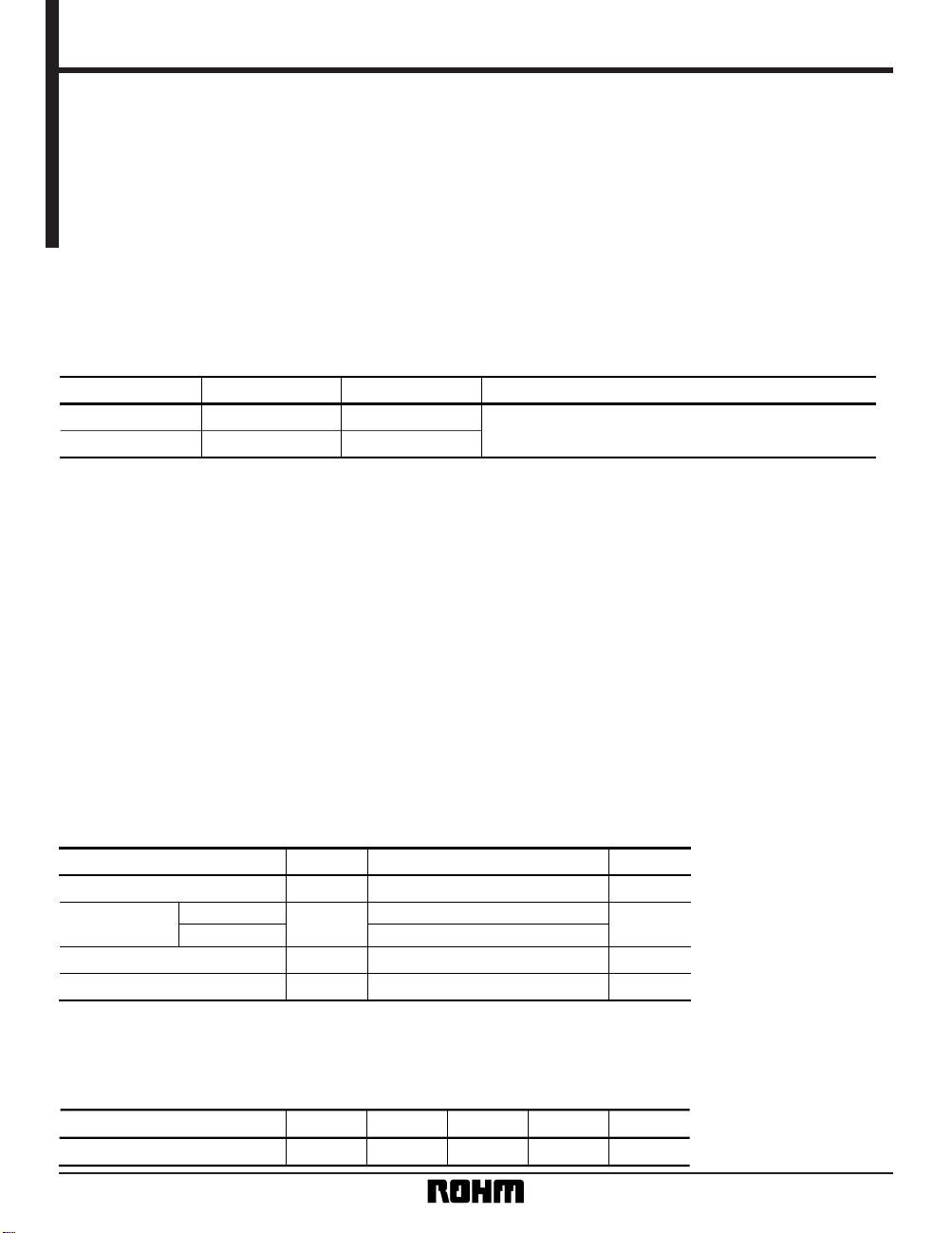
Block diagram
HP SUSPEND
SP SUSPEND
HP V
CC
SP V
CC
HP V
CC
HP OUT R
HP GND
SP IN L
SP IN R
HP OUT L
SP VCCLINE MIX ON / OFF
SP OUT1 R
SP OUT2 R
MONO / ST
SP GND
EVR CTRL
LINE IN L
MUTE CTRL
LINE IN R
BIAS
SYSTEM BEEP IN
LCH OUT
BEEP LEVEL
PM BEEP IN
SP OUT1 L
SP OUT2 L
HP SUSPEND
SP SUSPEND
1 2 3 4 5 6 7 8 9 10111213
141516171819
202122232425
VR VR
BA7786FP-Y
•
Pin descriptions
Pin No.
Pin name
Function
1
2
3
4
5
6
7
8
9
10
11
12
13
14
15
16
17
18
19
20
21
22
23
24
EVR CTRL
EVR control pin
25
Voltage
Type
— B (NPN)
LINE IN L
Line Lch input
2.5 B (PNP)
MUTE CTRL
Headphone mute control pin
5.0 100kΩ PULL UP
LINE IN R
Line Rch input
2.5 B (PNP)
BIAS
Bias
2.5 23.5kΩ
SYSTEM BEEP IN
SYSTEM BEEP input
2.5
B (NPN)
BEEP LEVEL
SYSTEM BEEP IN output level setting
4.2 C (PNP) ~ 3kΩ
LCH OUT
LINE IN L + SYSTEM BEEP IN output
— C (PNP)
PM BEEP IN
PM beep input
2.5 B (NPN)
SP OUT1 L
BTL speaker Lch output (forward)
2.5 EF (NPN)
SP OUT2 L
BTL speaker Lch output (reverse)
2.5 EF (NPN)
HP SUSPEND
Headphone SUSPEND control
5.0 100kΩ PULL UP
SP SUSPEND
Speaker SUSPEND control
5.0 100kΩ PULL UP
SP GND
Speaker ground
0.0 —
MONO / ST
Speaker amplifier Lch ON / OFF control
5.0 100kΩ PULL UP
SP OUT2 R
BTL speaker Rch output (reverse)
EF (NPN)
SP OUT1 R
BTL speaker Rch output (forward)
2.5 EF (NPN)
LINE MIX ON / OFF
SP IN L / R input ON / OFF control
5.0 100kΩ PULL UP
SP V
CC
Speaker Vcc
5.0 —
SP IN R
Speaker Rch input
2.5 B (NPN)
SP IN L
Speaker Lch input
2.5 B (NPN)
HP GND
Headphone ground
0.0 —
HP OUT R
Headphone Rch output
2.5 EF (NPN)
HP OUT L
Headphone Lch output
2.5
EF (NPN)
HP V
CC
Headphone Vcc
5.0 —
2.5
Note) The pin formats are as follows. EF: emitter follower; B: base; C: collector; ~ : series connection.
The above values are all based on the settings (HP V
CC = SP VCC = + 5.0V) in Fig. 1, entitled "Measurement circuit diagram,"
and do not guarantee standards.
BA7786FP-Y
Page 3
3
Multimedia ICs BA7786FP-Y / BA7787FS
•
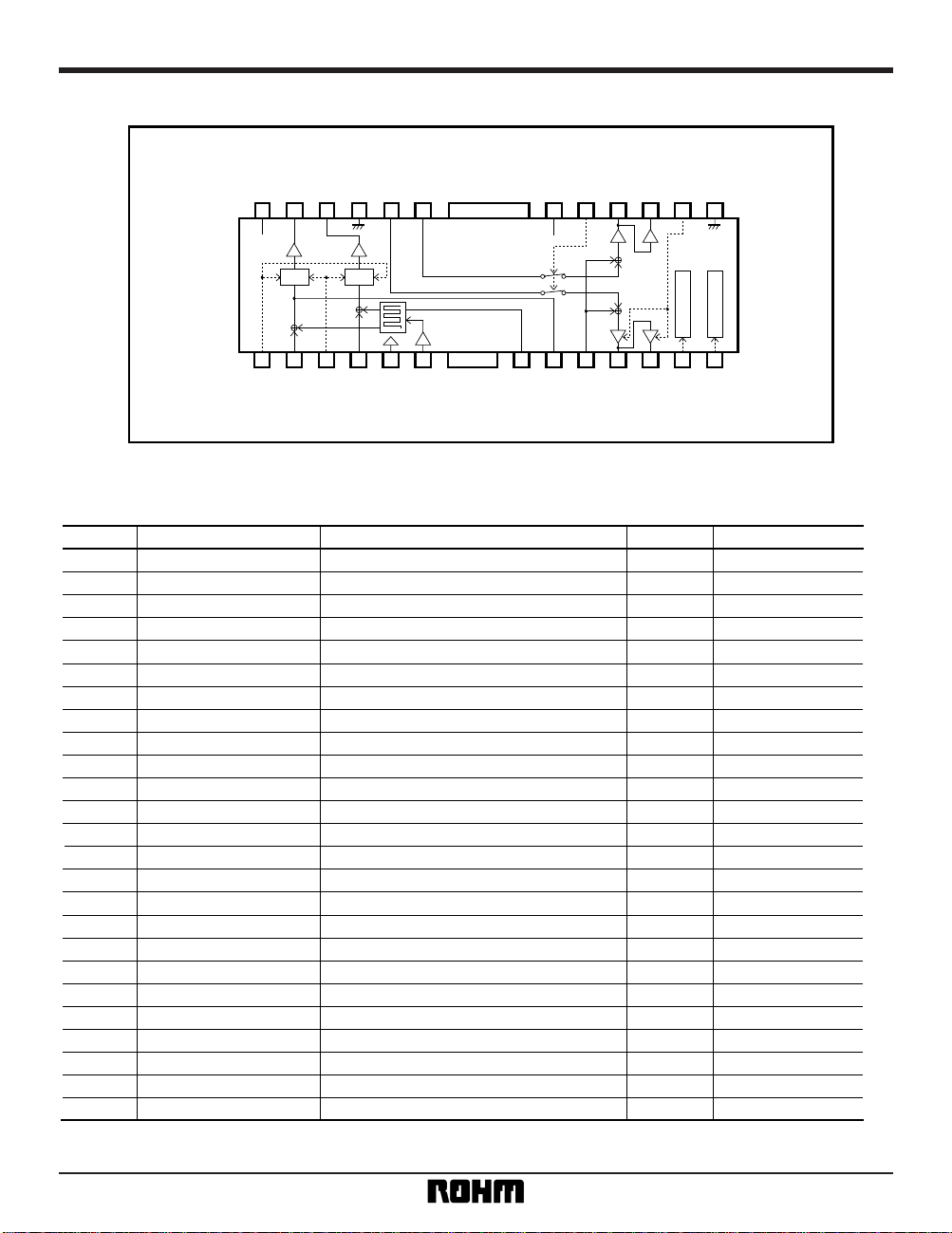
Block diagram
20 19 18 17 16 15 11
1 2 3 4 5 6 9 10
HP VCC
HP VCC
HP OUT R
HP GND
SP VCCBEEP LEVEL
HP OUT L
SP GND
EVR CTRL
LINE IN L
MUTE CTRL
LINE IN R
BIAS
SYSTEM BEEP IN
SP SUSPEND
HP SUSPEND
14
SP OUT113SP OUT212LINE MIX ON / OFF
7
SP IN
8
PM BEEP IN
SP VCC
HP SUSPEND
SP SUSPEND
VR VR
BA7787FS
1
EVR CTRL
EVR control pin
2
LINE IN L
Line Lch input
B (PNP)
B (PNP)
23.5kΩ
B (NPN)
B (NPN)
B (NPN)
B (PNP)
B (PNP)
EF (NPN)
EF (NPN)
EF (NPN)
—
—
EF (NPN)
—
B (NPN)
3
MUTE CTRL
Headphone mute control
100kΩ PULL UP
4
LINE IN R
Line Rch input
5
BIAS
Bias
6
SYSTEM BEEP IN
SYSTEM BEEP input
7
SP IN
Speaker input
8
PM BEEP IN
PM BEEP input
9
HP SUSPEND
Headphone SUSPEND control
10
SP SUSPEND
Speaker SUSPEND control
11
SP GND
Speaker ground
12
LINE MIX ON / OFF
SP IN input ON / OFF control
100kΩ PULL UP
C (PNP) ~ 3kΩ
13
SP OUT2
BTL speaker output (reverse)
14
SP OUT1
BTL speaker output (forward)
15
BEEP LEVEL
16
SP V
CC
Speaker Vcc
17
HP GND
Headphone ground
18
HP OUT R
Headphone Rch output
19
HP OUT L
Headphone Lch output
20
HP V
CC
Headphone Vcc
—
SYSTEM BEEP IN output level setting
Pin No. Pin name Function Pin voltage Pin type
—
2.5
5.0
2.5
2.5
2.5
2.5
2.5
—
—
0.0
5.0
2.5
2.5
4.2
5.0
0.0
2.5
2.5
5.0
Note) The pin formats are as follows. EF: emitter follower, B: base, C: collector, ~ : series connection.
The above values are all based on the settings (HP V
CC = SP VCC = + 5.0V) in Fig. 2, entitled "Measurement circuit diagram,"
and do not guarantee standards.
BA7787FS
Page 4
4
Multimedia ICs BA7786FP-Y / BA7787FS
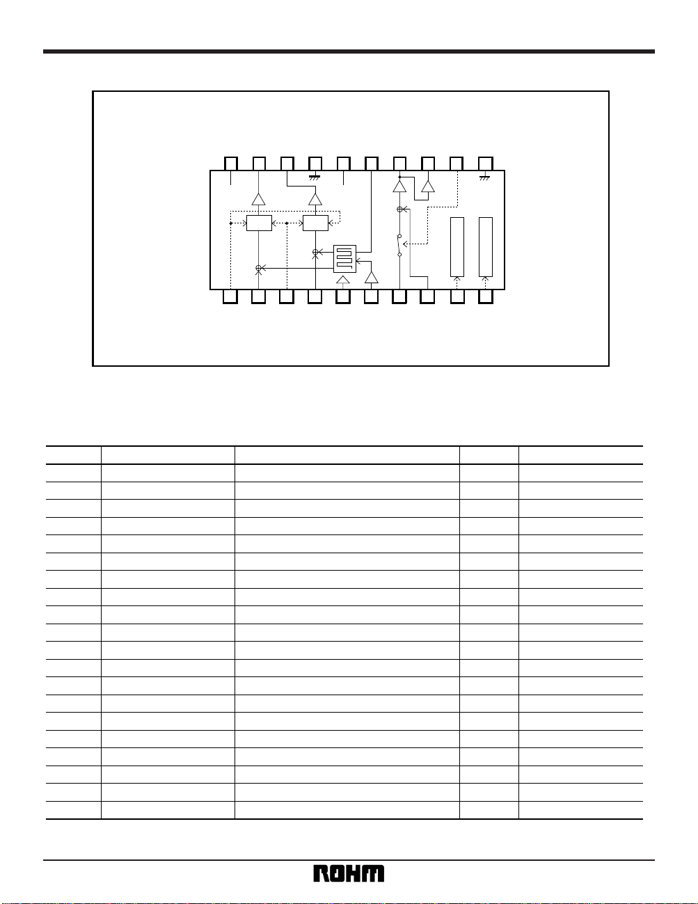
•
Control pin circuits
100k
3,15pin
10k
HP V
CC
BA7786FP-Y
MUTE CTRL (3pin)
MONO / ST (15pin)
100k
12,13pin
10k
HP V
CC
HP SUSPEND (12pin)
SP SUSPEND (12pin)
20k
100k
18pin
HP VCC
LINE MIX ON / OFF (18pin)
100k
3pin
10k
HP V
CC
BA7787FS
MUTE CTRL (3pin)
Note) All figures are design values, and do not represent guaranteed performance.
10k
9,10pin
HP V
CC
HP SUSPEND (9pin)
SP SUSPEND (10pin)
20k
100k
12pin
HP VCC
LINE MIX ON / OFF (12pin)
Page 5
5
Multimedia ICs BA7786FP-Y / BA7787FS
Parameter Symbol Unit ConditionsMin. Typ. Max.
〈Supply current〉
Supply current
Supply current SUSPEND
Output voltage level
Maximum output level
Output residual noise
Interchannel crosstalk
Muting level
Output voltage level
Input threshold level
Output voltage level
Distortion
Maximum output level
Output residual noise
Interchannel crosstalk
LINE MIX OFF level
Output level
〈MUTE CTRL〉 (pin 13)
HP MUTE ON holding voltage
HP MUTE OFF holding voltage
〈HP SUSPEND〉 (pin 12)
HP SUSPEND holding voltage
HP SUSPEND holding voltage
〈SP SUSPEND〉 (pin 13)
HP SUSPEND holding voltage
HP SUSPEND holding voltage
〈MONO / STEREO〉 (pin 15)
MONAURAL holding voltage
STEREO holding voltage
〈LINE MIX ON / OFF〉 (pin 18)
LINE MIX OFF holding voltage
LINE MIX ON holding voltage
EVR variation range
Distortion
Measurement circuit
3.52 4.82 7.64
No input, SP OUT = no load
Fig.1
I
CC
mA
175 240 410
No input, V
H = VS = H
Fig.1
I
CCS
µA
〈HP AMP 1〉 INPUT: LINE IN L / R, OUTPUT: HP OUT L / R
〈HP AMP 2〉 INPUT: SYSTEM BEEP IN, OUTPUT: HP OUT L / R
〈SP AMP 2〉 INPUT: PM BEEP IN, OUTPUT: SP OUT L / R
– 7.4 – 4.0 – 1.5
V
IN = – 10.0dBV
V
IN = – 10.0dBV
∗
1
VIN = – 10.0dBV
∗
2
VE = HP VCC→VE = ground level differential
Fig.1
V
OHP
dBV
— 0.1 1.0
Fig.1
THD
HP
%
– 1.6 + 0.6 —
THD = 1%
∗
1
Fig.1
V
OMHP
dBV
dBV
dBV
dBV
V
P-P
VP-P
dBV
70 90 —
Fig.1
G
EVR
dB
— – 80 – 73
R
g = 1kΩ
∗
2
VIN = – 7.0dBV
∗
2
VIN = – 7.0dBV
∗
2
, VM = L
V
IN = – 10.0dBV
V
IN = – 10.0dBV
∗
1
VIN = – 12.0dBV
∗
2
VIN = – 12.0dBV
∗
2
, VL = L
V
IN = – 10.0dBV
Fig.1
V
ONHP
— – 79 – 70
Fig.1
CT
HP
— – 94 – 83
Fig.1
MT
HP
0.22 0.32 0.42
V
IN = 5.0VP-P
Fig.1
4.5 — 5.0
Fig.1
V
HBH
VOSP
THDSP
VOHB
– 1.4 + 2.0 + 4.5
Fig.1
— 0.4 1.5
Fig.1
%
+ 3.5 + 5.7 —
THD = 1%
∗
1
Fig.1
V
OMSP
dBV
— – 90 – 80
R
g = 1kΩ
∗
2
Fig.1
V
ONSP
dBV
dBV
dBV
dBV
— – 78 – 70
Fig.1
CT
SP
— – 78
– 70
Fig.1
V
OOFFSP
– 7.4 – 4.0 – 1.5
Fig.1
Fig.1
Fig.1
VOSB
GND — 0.4VML V
4.3 — V
CCVMH V
GND — 0.4
Fig.1
V
HL V
4.3 — V
CC
Fig.1
V
HH V
4.3 — V
CC
Fig.1
V
SH V
GND — 0.4
Fig.1
V
SL V
4.3 — V
CC
Fig.1
V
NH V
GND — 0.4
Fig.1
V
NL
V
GND — 0.4
Fig.1
V
LL V
4.3 — V
CC
Fig.1
V
LH V
〈SP AMP 1〉 INPUT: SP IN L / R, OUTPUT: SP OUT L / R
∗
1: B.W. = 0.4 ~ 30kHz
∗
2: DIN audio mode settings are as follows, unless otherwise noted:
V
E = HP VCC (EVR = Max.), VM = H (HP MUTE OFF), VH = L (HP SUSPEND), VS = L (SP SUSPEND), VL = H (LINE MIX ON), VN = H (STEREO)
BA7786FP-Y
•
Electrical characteristics (unless otherwise noted, Ta = 25°C, HP VCC = SP VCC = 5.0V, f = 1kHz)
Page 6
6
Multimedia ICs BA7786FP-Y / BA7787FS
Parameter Symbol Unit ConditionsMin. Typ. Max.
〈Supply current〉
Supply current
Supply current SUSPEND
Output voltage level
Maximum output level
Output residual noise
Interchannel crosstalk
Muting level
Output voltage level
Input threshold level
Output voltage level
Distortion
Maximum output level
Output residual noise
Interchannel crosstalk
LINE MIX OFF level
Output level
〈MUTE CTRL〉 (pin 3)
HP MUTE ON holding voltage
HP MUTE OFF holding voltage
〈HP SUSPEND〉 (pin 9)
HP SUSPEND holding voltage
HP SUSPEND holding voltage
〈SP SUSPEND〉 (pin 10)
SP SUSPEND holding voltage
SP SUSPEND holding voltage
〈LINE MIX ON / OFF〉 (pin 12)
LINE MIX OFF holding voltage
LINE MIX ON holding voltage
EVR variation range
Distortion
Measurement circuit
3.10 4.25 6.74
No input, SP OUT = no load
Fig.2
I
CC
mA
175 240 410
No input, V
H = VS = H
Fig.2
I
CCS
µA
〈HP AMP 1〉 INPUT: LINE IN L / R, OUTPUT: HP OUT L / R
〈HP AMP 2〉 INPUT: SYSTEM BEEP IN, OUTPUT: HP OUT L / R
〈SP AMP 2〉 INPUT: PM BEEP IN, OUTPUT: SP OUT L / R
– 7.4 – 4.0 – 1.5
V
IN = – 10.0dBV
V
IN = – 10.0dBV
∗
1
VIN = – 10.0dBV
∗
2
VE = HP VCC→VE = ground level differential
Fig.2
V
OHP
dBV
— 0.1 1.0
Fig.2
THD
HP
%
– 1.6 + 0.6 —
THD = 1%
∗
1
Fig.2
V
OMHP
dBV
dBV
dBV
dBV
V
P-P
VP-P
dBV
70 90 —
Fig.2
G
EVR
dB
— – 80 – 73
R
g = 1kΩ
∗
2
VIN = – 7.0dBV
∗
2
VIN = – 7.0dBV
∗
2
, VM = L
V
IN = – 10.0dBV
V
IN = – 10.0dBV
∗
1
VIN = – 12.0dBV
∗
2
VIN = – 12.0dBV
∗
2
, VL = L
V
IN = – 10.0dBV
Fig.2
V
ONHP
— – 79 – 70
Fig.2
CT
HP
— – 94 – 83
Fig.2
MT
HP
0.22 0.32 0.42
V
IN = 5.0VP-P
Fig.2
4.5 — 5.0
Fig.2
V
HBH
VOSP
THDSP
VOHB
– 1.4 + 2.0 + 4.5
Fig.2
— 0.4 1.5
Fig.2
%
+ 3.5 + 5.7 —
THD = 1%
∗
1
Fig.2
V
OMSP
dBV
— – 90 – 80
R
g = 1kΩ
∗
2
Fig.2
V
ONSP
dBV
dBV
dBV
dBV
— – 78 – 70
Fig.2
CT
SP
— – 78
– 70
Fig.2
V
OOFFSP
– 7.4 – 4.0 – 1.5
Fig.2
Fig.2
Fig.2
VOSB
GND — 0.4VML V
4.3 — V
CCVMH V
GND — 0.4
Fig.2
V
HL V
4.3 — V
CC
Fig.2
V
HH V
4.3 — V
CC
Fig.2
V
SH V
GND — 0.4
Fig.2
V
SL V
GND — 0.4
Fig.2
V
LL V
4.3 —
—
—
—
—
—
—
—
—V
CC
Fig.2
V
LH V
〈SP AMP 1〉 INPUT: SP IN L / R, OUTPUT: SP OUT L / R
∗
1: B.W. = 0.4 ~ 30kHz
∗
2: DIN audio mode settings are as follows, unless otherwise noted:
V
E = HP VCC (EVR = Max.), VM = H (HP MUTE OFF), VH = L (HP SUSPEND), VS = L (SP SUSPEND), VL = H (LINE MIX ON),
V
N = H (STEREO)
BA7787FS
〈Control threshold voltage〉
Page 7
7
Multimedia ICs BA7786FP-Y / BA7787FS
1
25
24 23 21 20
19
18 17
16
15 14
2
3
456
8
7
9
10 11 12 13
22
VR
HP SUSPEND
27k
27k
27k
18k
8
33k
390k
0.47µ
47µ
47µ
100
100
8
1k
15k
15k
1k
0.47µ
0.47µ
0.47µ
0.47µ
0.47µ
22µ
1µ
1k
1k
1k
1k
SP SUSPEND
VR
BA7786FP-Y
HP VCC
SP VCC
HP OUT R
HP GND
SP IN L
SP IN R
HP OUT L
SP OUT R
SP GND
LINE IN L
LINE IN R
SYSTEM BEEP IN
LCH OUT
PM BEEP IN
SP OUT L
HP VCC
SP VCC
VL
VE
VM
VH
VS
VN
Fig. 1
+ +
+
+
+
+
•
Measurement circuit
Page 8
8
Multimedia ICs BA7786FP-Y / BA7787FS
1
20
19 18
16
15
14
13 12
11
2
3456 8
7
9
10
17
VR
HP SUSPEND
V
E
VL
27k
27k
33k
0.47µ
47µ
47µ
100
100
8
390k
0.47µ
0.47µ
22µ
1k
1k
1k
V
M
VH
VS
SP SUSPEND
15k
0.47µ
1k
18k
0.47µ
1k
VR
BA7787FS
HP VCC
HP VCC
HP OUT R
HP GND
SP V
CC
HP OUT L
SP GND
LINE IN L
LINE IN R
SYSTEM BEEP IN
SP OUT
SP IN
PM BEEP IN
SP VCC
Fig. 2
+ +
+
+
+
Page 9

9
Multimedia ICs BA7786FP-Y / BA7787FS
•
Circuit operation
(1) Gain between LINE IN L / LINE IN R and HP OUT L /
HP OUT R
G
HP, the gain when EVR is at its maximum (VE = HP
V
CC), is calculated as follows:
(2) Output level between SYSTEM BEEP IN and HP
OUT L / HP OUT R
Inputting a pulse wave to SYSTEM BEEP IN causes HP
OUT L and HP OUT R to output a pulse wave. The output level of this pulse wave depends on the resistance
between pin 7 and GND. The level when EVR is at its
maximum (V
E = HP VCC) is calculated as follows.
(4) Gain between PM BEEP IN and SP OUT 1 / SP OUT 2
This is calculated as follows.
(BA7786FP-Y only, BA7787FS: pin 8)
This path is output regardless of whether LIN MIX ON /
OFF is at the high or low level.
(3) Gain between SP IN L / SP IN R and SP OUT L / SP
OUT R (BA7786FP-Y)
This is calculated as follows.
This path is not controlled by EVR or the mute function.
(5) Gain between LINE IN L and LCH OUT
(BA7786FP-Y)
This gain (G
HL) is calculated as follows.
Set so that 12k ⬉ R ⬉ 56k. This gain attenuates according to the pin 1 DC voltage (V
E) (see Fig. 8). Mixing
input can be accommodated by attaching multiple resistors.
Gain between SP IN and SP OUT 1 / SP OUT 2
(BA7787FS)
This is calculated as follows.
Set so that R ⭌ 100k (V
HB ⬉ 1.1V). As with the path be-
tween LINE IN L / LINE IN R and HP OUT L / HP OUT
R, this level attenuates according to the pin 1 DC voltage.
(BA7786FP-Y only, BA7787FS: pin 15)
2
R
4
R
20
21
R
R
7
R
9
R
7
R
GHP ⱌ 20 ∗ LOG (dB)
60k
1k + R
GSP ⱌ 20 ∗ LOG (dB)
32k
1k + R
GSP ⱌ 20 ∗ LOG (dB)
32k
1k + R
GSB ⱌ 20 ∗ LOG (dB)
20k
1k + R
GHL ⱌ 20 ∗ LOG (dB)
R8
2 ∗ R2
VHB ⱌ 0.5 ∗ ∗ 60k (VP-P)
V
CC – 0.7
13k + R
2
R8
8
R2
Page 10

10
Multimedia ICs BA7786FP-Y / BA7787FS
(6) Output level between SYSTEM BEEP IN and LCH
OUT (BA7786FP-Y)
Inputting a pulse wave to SYSTEM BEEP IN causes
LCH OUT to output a pulse wave. The output level of
this pulse wave depends on the resistance between pin
7 and GND and between pin 8 and GND, and is calculated as follows.
(7) EVR control characteristics
The headphone amplifier is controlled by changing the
resistive potential division ratio.
This path is not controlled by EVR or the mute function.
8
7
R7
R8
VHS ⱌ 0.25 ∗ ∗ R8 (VP-P)
V
CC – 0.7
13k + R7
Page 11

11
Multimedia ICs BA7786FP-Y / BA7787FS
•
Control pins
(1) MUTE CTRL
• Turns the headphone mute function on and off.
(3) SP SUSPEND
• Turns the speaker suspend function on and off.
(2) HP SUSPEND
• Turns the headphone suspend function on and off.
• Because the BA7786FP-Y has a pull-up resistor, this is possible even when open (if at the high level).
• Because the BA7786FP-Y has a pull-up resistor, this is possible even when open (if at the high level).
Control signal: VM Note
—
HP MUTE ON L Turns off HP AMP output
HP MUTE OFF H (OPEN)
Control signal: VH Note
HP SUSPEND
L
H
The headphone amplifier operates
The headphone amplifier turns offHP SUSPEND
Control signal: VS Note
SP SUSPEND
L
H
The speaker amplifier operates
The speaker amplifier turns offSP SUSPEND
(4) LINE MIX ON / OFF
• Turns the SP IN input on and off according to SP OUT.
Control signal: VL Note
—
LINE MIX OFF
L
H (OPEN)
Stops the output of SP IN input to SP OUT
LINE MIX ON
(5) MONO / STEREO (BA7786FP-Y)
• Turns SP AMP LCH on and off.
Control signal: VN Note
SP AMP LCH OFF
L
H (OPEN)
SP AMP LCH turns off
SP AMP LCH ON
SP AMP LCH operates
Page 12

12
Multimedia ICs BA7786FP-Y / BA7787FS
HP SUSPEND
SP SUSPEND
HP VCC
SP VCC
HP VCC
SP VCC
HP GND
SPSP
MONO / ST
EVR CTRL
BEEP LEVEL
LINE IN L
MUTE CTRL
LINE IN R
BIAS
SYSTEM BEEP IN
LCH OUT
PM BEEP IN
HP SUSPEND
SP SUSPEND
SP GND
1
2
3
4
5
6
8
9
10
11
12
19
18
17
16
15
14
25
24
23
22
21
20
7
100
27k
∗
VR
V
CC
HP JACK
15k 15k
100
27k
∗
33k
390k
27k
8Ω
∗
8Ω
∗
is for mixing input.
Fig. 3
13
VR
VR
+
+
+
+
+
•
Application example
BA7786FP-Y
Pin
No.
TERMINAL
NAME
FUNCTION
L
H
TERMINAL
FORM
3
12
13
15
18
MUTE CTRL
HP SUSPEND
SP SUSPEND
MONO / ST
LINE MIX ON / OFF
HP MUTE ON
HP OPERATED
SP OPERATED
LCH SP OFF
LINE MIX OFF
HP MUTE OFF
HP SUSPENDED
LCH SP ON
LINE MIX ON
SP SUSPENDED
100k PULL UP
100k PULL UP
100k PULL UP
100k PULL UP
100k PULL UP
Page 13

13
Multimedia ICs BA7786FP-Y / BA7787FS
HP VCC
SP VCC
HP SUSPEND
SP SUSPEND
1
2
3
4
5
20
19
18
17
16
6
7
8
9
10
15
14
13
12
11
HP V
CC
HP GND
SP VCC
100
HP JACK
100
390k
8Ω
SP
SP GND
EVR CTRL
MUTE CTRL
LINE IN R
LINE IN L
SYSTEM BEEP IN
27k
27k
15k
18k
15k
33k
VR
V
CC
PM BEEP IN
HP SUSPEND
SP SUSPEND
BIAS
∗
is for mixing input
Fig. 4
VR
VR
∗
∗
∗
+
+
+
+
+
BA7787FS
Pin
No.
TERMINAL
NAME
FUNCTION
L
H
TERMINAL
FORM
3
9
10
12
MUTE CTRL
HP SUSPEND
SP SUSPEND
LINE MIX ON / OFF
HP MUTE ON
HP OPERATED
SP OPERATED
LINE MIX OFF
HP MUTE OFF
HP SUSPENDED
LINE MIX ON
SP SUSPENDED
100k PULL UP
PNP BASE
PNP BASE
100k PULL UP
Page 14

14
Multimedia ICs BA7786FP-Y / BA7787FS
INPUT: LINE IN L
OUTPUT: HP OUT L
V
IN = – 30dBV
HP V
CC = 5.0V
SP V
CC = 5.0V
V
E = 5.0V
100 100k10k1k 1M 10M
– 20
OUTPUT LEVEL: VO (dBV)
PHASE (deg)
FREQUENCY: f (Hz)
– 30
– 40
– 50
– 60
– 70
– 80
– 90
– 100
– 180
+ 180
Fig. 5 HP AMP frequency
characteristics
•
Electrical characteristic curves
INPUT: LINE IN L
OUTPUT: HP OUT L
f = 1kHz
HP V
CC = 5.0V
SP
VCC = 5.0V
V
E = 5.0V
B.W. = 0.4 ~ 30kHz
RL = 100Ω
RL = ∞
– 40 – 10– 20– 30 0
OUTPUT DISTORTION: THD (%)
INPUT LEVEL: VIN (dBV)
10
1
0.1
0.01
Fig. 6 HP AMP input level vs.
output distortion
INPUT: LINE IN L
OUTPUT: HP OUT L
V
IN = – 6.4dBV
HP V
CC = 5.0V
SP V
CC = 5.0V
V
E = 5.0V
DIN AUDIO
VM = GND
VM = 5.0V
10 1k100 10k 100k
10
0
OUTPUT LEVEL: VO (dBV)
FREQUENCY: f (Hz)
– 10
– 20
– 30
– 40
– 50
– 60
– 70
– 90
– 80
– 100
Fig. 7 HP AMP MUTE
characteirstics
INPUT: LINE IN L
OUTPUT: HP OUT L
V
IN = – 10dBV, f = 1kHz
HP V
CC = 5.0V
SP V
CC = 5.0V
DIN AUDIO
0 0.5 1.0
0
OUTPUT LEVEL: VO (dBV)
VOLTAGE RATIO: VE / VCC
– 50
– 100
Fig. 8 HP AMP EVR
characteristics
INPUT: LINE IN L
OUTPUT: HP OUT L
V
IN = 5.0Vpp, f = 10kHz
HP V
CC = 5.0V
SP V
CC = 5.0V
V
E = 5.0V
10k 100k 1M
OUTPUT LEVEL: VO (Vpp)
BA7787FS: 15pin
BA7786FP-Y: 7pin
RESISTOR: R (Ω)
1.0
0.1
Fig. 9 SYSTEM BEEP output level vs.
external resistor.
INPUT: SP IN
OUTPUT: SP OUT 1
V
IN = – 30dBV
HP V
CC = 5.0V
SP V
CC = 5.0V
100 100k10k1k 1M 10M
– 20
OUTPUT LEVEL: VO (dBV)
FREQUENCY: f (Hz)
– 100
Fig.10 SP AMP frequency
characteristics
INPUT: SP IN
OUTPUT: SP OUT 1 / 2, f = 1kHz
HP V
CC = 5.0V, SP VCC = 5.0V
V
E = 5.0V, B.W. = 0.4 ~ 30kHz
RL = ∞
RL = 8Ω
– 50 – 10– 20– 30– 40 0
OUTPUT DISTORTION: THD (%)
INPUT LEVEL: VIN (dBV)
10
1
0.1
0.01
Fig. 11 SP AMP input level vs.
output distortion
RL = speaker (8Ω)
INPUT: SP IN
OUTPUT: SP OUT 1 / 2
V
IN = – 11.6dBV
HP V
CC = 5.0V
SP V
CC = 5.0V
DIN AUDIO
10 1k100 10k 100k
10
0
OUTPUT LEVEL: VO (dBV)
FREQUENCY: f (Hz)
– 10
– 20
– 30
– 40
– 60
– 50
– 70
– 80
– 90
– 100
Fig. 12 SP AMP MUTE
characteristics
VL = GND
VL = 5.0V
Page 15

15
Multimedia ICs BA7786FP-Y / BA7787FS
HP SUSPEND
SP SUSPEND
HP VCC
SP VCC
HP VCC
SP VCC
HP GND
LINE IN L
MUTE
LINE IN R
BIAS
SYSTEM BEEP IN
LCH OUT
BEEP LEVEL
PM BEEP IN
SP OUT1 L
SP OUT2 L
HP SUS
SP SUS
HP V
CC
LCH ON / OFF
MIX ON / OFF
SP GND
1
2
3
4
5
6
8
9
10
11
12
19
18
17
16
15
14
25
24
23
22
21
20
7
R17
R14
R15
100
100µ
47µ
47µ
C11
C1
0.1µ
0.1µ
C2
C4
0.1µ
C5
0.1µ
C6
0.1µ
47µ
C3
C10
C9
C14
C13
C12
C7
C8
0.1µ
100µ
0.1µ
1
2
3
0.1µ
0.1µ
27k
VR1
R1
R2
R3
R4
R5
R6
R7
R8
R9
V
CC
HP JACK
HP OUT L
HP GND
HP OUT R
HP GND
15k
R16
15k
100
27k
33k
390k
R10
18k
18k
27k
R11
R13
SP OUT1 R
SP OUT2 R
Fig. 13
13
VR
VR
+
+
++
+
•
Board circuit
BA7786FP-Y
Page 16

16
Multimedia ICs BA7786FP-Y / BA7787FS
HP VCC
SP VCC
1
2
3
4
5
20
19
18
17
16
6
7
8
9
10
15
14
13
12
11
SP V
CC
BEEP LEVEL
HP GND
HP V
CC
HP VCC
HP GND
HP GND
HP OUT L
HP OUT R
HP GND
GND
R15
100
R14
100
C12
C10
C11
C1
C3
C7
C8
47µ
47µ
47µ
C9
100µ
0.1µ
0.1µ
0.1µ
0.1µ
C2
0.1µ
C4
C5
C6
0.1µ
100µ
0.1µ
HP JACK
R13
390k
SP GND
LINE IN L
27k
27k
15k
18k
15k
33k
VR1
BIAS
SP GND
SP OUT1
SP OUT2
1
2
3
R1
R2
R3
R4
R5
R6
R7
R8
R9
R10
R11
R12
GND
LINE IN R
GND
GND
SYSTEM BEEP IN
PM BEEP IN
MUTE
HP SUS
SP SUS
MIX ON / OFF
Fig. 14
HP SUSPEND
SP SUSPEND
VR
VR
+
++
+
+
BA7787FS
Page 17

17
Multimedia ICs BA7786FP-Y / BA7787FS
No.
Use
Standard value
R1
Used to set the gain from LINE IN L / LINE IN R (pins 2 and 4) to HP OUT
L / HP OUT R (pins 24 and 23)
27kΩ
R2
(See section 1, on circuit operation for the formula.)
27kΩ
R3
A wide range of mixing ratios can be set by changing the values of
27kΩ
R4
R1, R2 and R3 (or R4, R5 and R6).
27kΩ
R5
27kΩ
R6
27kΩ
R7
33kΩ
R8
33kΩ
R9
33kΩ
R10
Used to set the output level from SYSTEM BEEP IN (pin 6) to HP OUT
L / HP OUT R (pins 24 and 23). (See section 2, on circuit operation for the formula.)
390kΩ
R11
• No need to attach. Connect pin 8 to a ground.
—
R13
• Used to set the gain from PM BEEN IN (pin 9) to SP OUT L / SP OUT R
(pins 10, 11, 16 and 17). (See section 4, on circuit operation for the formula.)
18kΩ
R14
R15
• The load resistor for HP OUT R.
100Ω
• The load resistor for HP OUT L.
100Ω
Used to set the gain from SP IN L / R (pins 21 and 20) to SP OUT L / R (pins 10, 11,
16 and 17). (See section 3, on circuit operation for the formula.)
15kΩ
R17
R16
15kΩ
C1
• The coupling capacitor for LINE IN L
0.1µF
C2
• The coupling capacitor for LINE IN R
0.1µF
C3
• The ripple rejection capacitor for the bias pin
47µF
C4
• The coupling capacitor for SYSTEM BEEP IN
0.1µF
C5
• No need to attach
—
C6
• The coupling capacitor for PM BEEP IN
0.1µF
C7
• The bypass capacitor for SP V
CC (used for low-frequency ripple rejection)
100µF
C8
• The bypass capacitor for SP V
CC (used for high-frequency ripple rejection)
0.1µF
C9
• The coupling capacitor for HP OUT R
47µF
C10
• The coupling capacitor for HP OUT L
47µF
C11
• The bypass capacitor for HP V
CC (used for low-frequency ripple rejection)
100µF
C12
• The bypass capacitor for HP V
CC (used for high-frequency ripple rejection)
0.1µF
C13
• The coupling capacitor for SP IN R
0.1µF
C14
• The coupling capacitor for SP IN L
0.1µF
VR1
• Used to change the pin 1 DC voltage
20kΩ
BA7786FP-Y
Resistors for mixing SYSTEM BEEP IN (pin 6). Because the threshold voltage
between the high and low levels is fixed inside the IC, these resistors should be
set to 33kΩ
•
Part table
Page 18

18
Multimedia ICs BA7786FP-Y / BA7787FS
No.
Use
Standard value
R1
Used to set the gain from LINE IN L / LINE IN R (pins 2 and 4) to HP OUT
L / HP OUT R (pins 19 and 18) (See section 1, on circuit operation for the formula.)
27kΩ
R2
27kΩ
R3
A wide range of mixing ratios can be set by changing the values of R1, R2 and
R3 (or R4, R5 and R6).
27kΩ
R4
27kΩ
R5
27kΩ
R6
27kΩ
R7
33kΩ
R8
33kΩ
R9
33kΩ
R10
• Used to set the gain from SP IN (pin 7) to SP OUT 1 / SP OUT 2
(pins 14 and 13). (See section 3, on circuit operation for the formula.)
• Used to set the output level from SYSTEM BEEP IN (pin 6) to HP OUT
L / HP OUT R (pins 19 and 18).
(See section 2, on circuit operation for the formula.)
15kΩ
15kΩ
18kΩ
390kΩ
R12
R11
R13
• Used to set the gain from PM BEEP IN (pin 8) to SP OUT 1 / SP OUT 2
(pins 14 and 13).
R14
• The load resistor for HP OUT R.
100Ω
• The load resistor for HP OUT L.
100Ω
R15
20kΩ
C1
• The coupling capacitor for LINE IN L
0.1µF
C2
• The coupling capacitor for LINE IN R
0.1µF
C3
• The ripple rejection capacitor for the bias pin
47µF
C4
• The coupling capacitor for SYSTEM BEEP IN
0.1µF
C5
0.1µF
C6
• The coupling capacitor for PM BEEP IN
• The coupling capacitor for SP IN
0.1µF
C7
• The bypass capacitor for SP V
CC (used for low-frequency ripple rejection)
100µF
C8
• The bypass capacitor for SP V
CC (used for high-frequency ripple rejection)
0.1µF
0.1µF
C9
• The coupling capacitor for HP OUT R
47µF
C10
• The coupling capacitor for HP OUT L
47µF
C11
C12
VR1
• The bypass capacitor for HP V
CC (used for low-frequency ripple rejection)
• The bypass capacitor for HP V
CC (used for high-frequency ripple rejection)
• Used to change the pin 1 DC voltage
100µF
BA7787FS
(See section 4, on circuit operation for the formula.)
Resistors for mixing SYSTEM BEEP IN (pin 6). Because the threshold voltage
between the high and low levels is fixed inside the IC, these resistors should be set
to 33kΩ.
Page 19

19
Multimedia ICs BA7786FP-Y / BA7787FS
•
Operation notes
(1) Popping noises occurring when the power is turned
on
• When the power is turned on, the headphone mute
function should be on and the suspend function off in
order to prevent popping noises from occurring when
V
CC turns on.
(2) The supply voltages for HP V
CC and SP VCC should
come from the same power supply. Using separate
power supplies can lead to output voltage drops and
malfunctioning.
(3) The common impedance of the two power supply
lines (HP V
CC and SP VCC) should be kept as low as
possible.
(4) Make sure the input resistance for the SYSTEM
BEEP IN pin is 33kΩ.
(5) Configure the PM BEEP IN pin of BA7786FP-Y as
shown below in order to prevent oscillation in the IC.
(6) The LCH OUT pin (pin 8) of BA7786FP-Y should be
grounded when not used.
(7) When switching the suspend function popping noises may occur. If this bothers, take measures for eliminating it by attachig external componets.
33k
Page 20

20
Multimedia ICs BA7786FP-Y / BA7787FS
MIX
LCH
ON /
OFF
SP
SUS
HP
SUS
MUTE
SP
OUT1
L
SP
OUT2
L
ON /
OFF
J11
J12
J1
J2
J3
J4
J10
J9
J8
J5
G PM
BEEP IN
G SYSTEM
BEEP IN
GND LINE IN
R
GND LINE IN
L
1
3
2
SP
OUT2
R
SP
OUT1
R
SP
GND
SP
V
CC
LCH
OUT G
R13
R11
R12
R10
R9
R8
R7
R6
R5
R4
R1R2R3
C1
C2
C3
C11
C12
VR1
R15
R14
C10 C9
14 25
13 1
C8
C7
C5
C14
C13
C6
C4
R17
R16
J6
J7
HP
V
CC
HP
GND
HP R
GND
HP
OUT R
HP
OUT L
HP L
GND
TO HEADPHONE JACK
APB-BA7786FP-Y
Fig. 15
•
Board labelling diagram
BA7786FP-Y
LINE IN L: Line input Lch
LINE IN R: Line input Rch
SYSTEM BEEP IN: System beep sound input
PM BEEP IN: PM beep sound input
HP OUT L: Headphone output Lch monitor
HP OUT R: Headphone output Rch monitor
SP OUT L 1 / 2: Speaker connection pin (BTL)
SP OUT R 1 / 2: Speaker connection pin (BTL)
SP V
CC: Supply voltage input + 5.0V
HP V
CC: Supply voltage input + 5.0V
VR1: Electric volume adjuster va
(On this board, G
HP is set to its maximum by turning
the volume adjuster clockwise as far as it will go.)
MUTE: MUTE control switch
HP SUS: HP suspend control switch
SP SUS: SP suspend control switch
MIX ON / OFF: LINE MIX ON / OFF switch
(On this board, pin 12 automatically drops to the
ground level when a headphone is plugged into the
jack.)
LCH ON / OFF: SP AMP LCH ON / OFF switch
Page 21

21
Multimedia ICs BA7786FP-Y / BA7787FS
Fig. 16
•
Board pattern diagram
BA7786FP-Y
Page 22

22
Multimedia ICs BA7786FP-Y / BA7787FS
MIX
SP
SUS
HP
SUS
MUTE
ON /
OFF
J1
J2
J3
J4
J8
J5
G PM
BEEP IN
G SYSTEM
BEEP IN
GND LINE IN
R
GND LINE IN
L
1
3
2
SP
OUT2
SP
OUT1
SP
GND
SP
V
CC
R9
R8
R7
R6
R5
R4
R3
C11
C12
VR1
R15
R14
C10
11 20
10 1
C8
C7
R13
C6
HP
V
CC
HP
GND
HP R
GND
HP
OUT R
HP
OUT L
HP L
GND
TO HEADPHONE JACK
C9
R12
J7
J6
C5
C4
C3
C2
C1
APB-BA7787FS
R2
R1
R10
R11
Fig. 17
•
Board labelling diagram
BA7787FS
LINE IN L: Line input Lch
LINE IN R: Line input Rch
SYSTEM BEEP IN: System beep sound input
PM BEEP IN: PM beep sound input
HP OUT L: Headphone output Lch monitor
HP OUT R: Headphone output Rch monitor
SP OUT 1: Speaker connection pin (BTL)
SP OUT 2: Speaker connection pin (BTL)
SP V
CC: Supply voltage input + 5.0V
HP V
CC: Supply voltage input + 5.0V
VR1: Electric volume adjuster va
(On this board, G
HP is set to its maximum by turning
the volume adjuster clockwise as far as it will go.)
MUTE: MUTE control switch
HP SUS: HP suspend control switch
SP SUS: SP suspend control switch
MIX ON / OFF: LINE MIX ON / OFF switch
(On this board, pin 12 automatically drops to the
ground level when a headphone is plugged into the
jack.)
Page 23

23
Multimedia ICs BA7786FP-Y / BA7787FS
Fig. 18
•
Board pattern diagram
BA7787FS
Page 24

24
Multimedia ICs BA7786FP-Y / BA7787FS
HSOP25
BA7786FP-Y BA7787FS
SSOP-A20
7.8 ± 0.3
5.4 ± 0.2
2.75 ± 0.1
1.95 ± 0.1
25 14
1
13
0.11
1.9 ± 0.1
0.36 ± 0.1
0.3Min.
0.25 ± 0.1
13.6 ± 0.2
0.8
0.15
11
10
20
1
0.11
7.8 ± 0.3
5.4 ± 0.2
8.7 ± 0.2
0.15 ± 0.1
0.36 ± 0.10.8
1.8 ± 0.1
0.3Min.
0.15
•
External dimensions (Units: mm)
 Loading...