

Page 1
1
Video ICs
Stereo microphone amplifier for camcorders
BA7781K
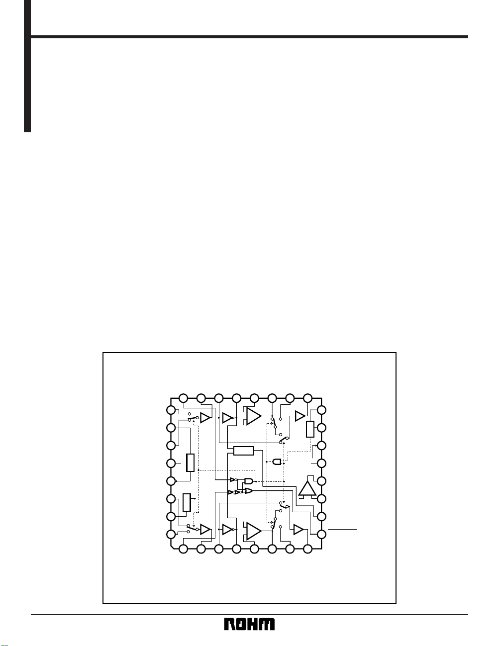
The BA7781K allows construction of a stereo-microphone amplifier for camcorder use with a minimum number of
external components. The IC has a built-in wind-noise detection circuit, and wind-noise rejection filter. The filter circuit is controlled automatically. The IC can operate off a 3.0V power supply.
•
Applications
Camcorders
•
Features
1) Operates off a 3.0V to 5.25V power supply.
2) Automatic wind-noise rejection circuit.
3) Matrix circuit for stereo emphasis.
4) Automatic switching circuit for external microphones, built-in external monaural decision circuit,
and input switch mode decision circuit.
•
Block diagram
04 05 06
24
23
22
18 17
16
15
14
12
11
09
25
26
27
28
29
30
31
32
13
10
01
02
03 07 08
21 20 19
EXT IN L
BG
INT IN L
GND
VREG
INT IN R
RIPL
EXT IN R
DET OUT
DET IN
BIAS
V
CC
LPF INV OUT
LPF INV IN
MIX OUT
MIC MONO
MODE 24
PRE OUT L
INV IN L
INV OUT L
MTX IN L
MTX OUT L
HPF IN L
OUT L
MODE 1
PRE OUT R
INV IN R
INV OUT R
MTX IN R
MTX OUT R
HPF IN R
OUT R
EXT
INT
13dB
13dB
GND
REG
BIAS
INT
EXT
+
–
NOR
WND
NOR
WND
15dB
–
EXT
EXT
BIAS
V
CC
MIX
+
–
10dB
15dB
–
+
DET
+
Page 2
2
Video ICs BA7781K
•
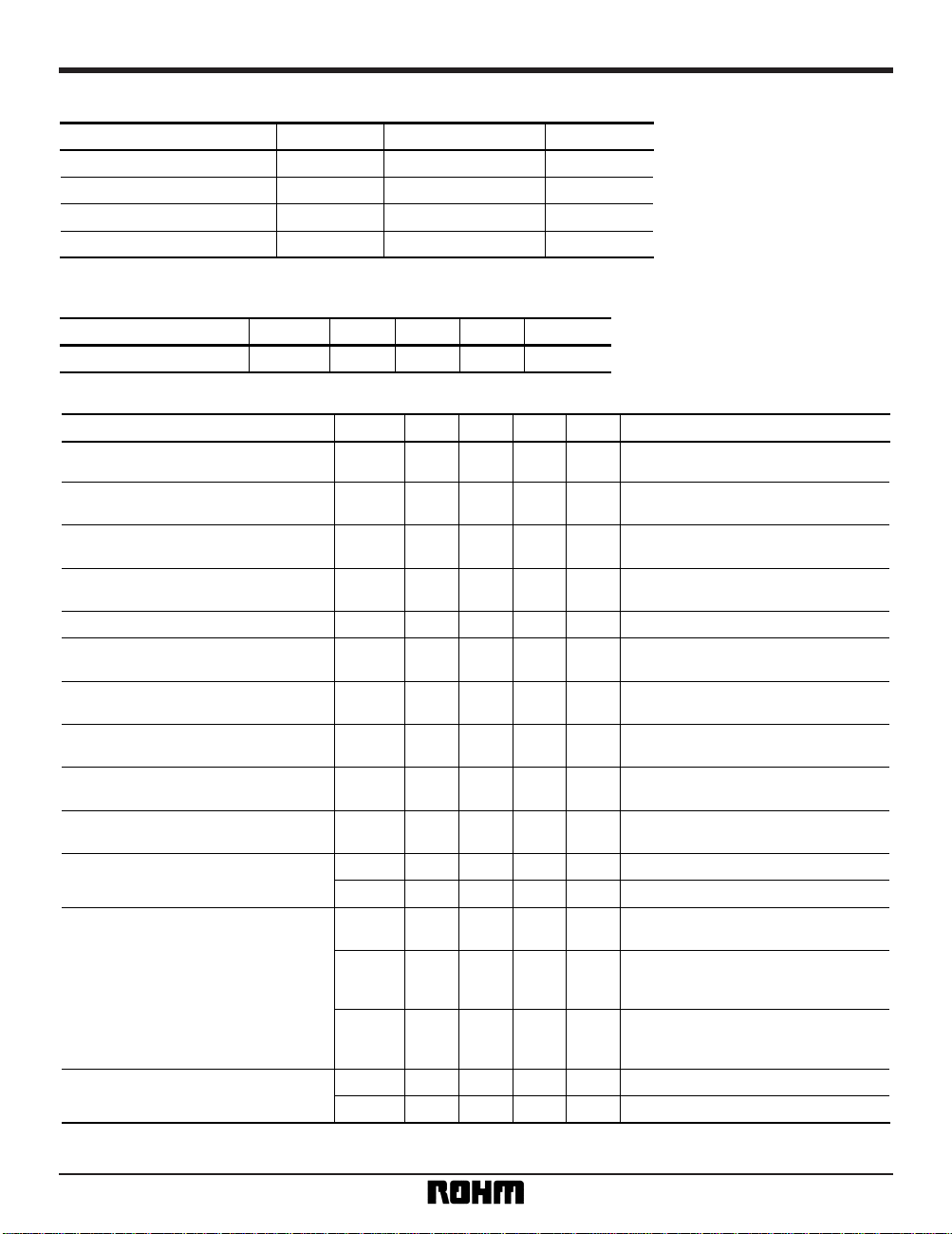
Absolute maximum ratings (Ta = 25°C)
Parameter
Symbol Limits Unit
V
CC
7.0 V
Pd mW
Topr °C
Tstg °C
400
∗
– 10 ~ +70
– 55 ~ +125
∗
Reduced by 4mW for each increase in Ta of 1°C over 25°C.
Power supply voltage
Power dissipation
Operating temperature
Storage temperature
•
Recommended operating conditions (Ta = 25°C)
Parameter Symbol Min. Typ. Max. Unit
V
CCS
3.0 — 5.25 VPower supply voltage
•
Electrical characteristics (unless otherwise noted, Ta = 25°C and VCC = 3.3V)
Parameter
Symbol Min. Typ. Max. Unit
I
INT
— 5.0 8.0 mA
I
EXT
— 4.8 8.0 mA
VG
PR
12 13 14 dB
VG
OA
14 15 16 dB
THD — 0.05 0.3 %
V
om 0.85 1.1 — Vrms
VNO — – 90 – 80 dBV
CT
I
→E
— – 88 – 70 dB
— – 61 – 50 dB
V
REG
2.3 2.5 2.75 V
V
HSWH
1.6 — VCC V
V
HSWL
0 — 0.6 V
VG
HON
— — – 30 dB
VG
HOFF
— — – 30 dB
V
HON
2.5 — V
V
HOFF
0 — 0.3 V
CT
L←
→R
Conditions
V
CC
INT MIC IN, L / Rch
EXT MIC IN, L / Rch
30 / 32pin→2pin GAIN
27 / 25pin→23pin GAIN
3 / 6 / 7pin→8pin GAIN
22 / 19 / 18pin→17pin GAIN
INT / EXT, Vo = 300mV
rms, L / Rch
∗
2
INT / EXT MIC IN, L / Rch
INT / EXT, L / Rch, R
g = 1kΩ
INT / EXT MIC, Lch→Rch, R
g = 1kΩ
15pin – 29.0dBV IN (80Hz)
6 / 19pin – 25.5dBV IN (1kHz)
6→8pin / 19→17pin GAIN
15pin – 45.0dBV IN (80Hz)
7 / 18pin – 25.5dBV IN (1kHz)
7→8pin / 18→17pin GAIN
INT→EXT MIC IN, R
g = 1kΩ, L / Rch
Current dissipation 1
Current dissipation 2
Preamplifier gain
Output amplifier gain
Distortion
Maximum output voltage
Output noise voltage
Input switch separation
Interchannel separation
Internal microphone power supply voltage
Input switch control voltage
High-pass filter switching
attenuation characteristic
High-pass filter control voltage
∗
1 JIS-A filter used.
∗
2 400Hz to 30kHz filter used.
No dissipation by mic
No dissipation by mic
f = 1kHz (distortion 1%
∗
2
)
When gain is 28dB
∗
1
(distortion 1%
∗
2
) , when gain is 28dB
∗
1
(distortion 1%
∗
2
) , when gain is 28dB
∗
1
Pin 27 output voltage for 30kΩ load
“H”level, 1 / 24 pin DC
“L” level, 1 / 24 pin DC
Input 80Hz signal to pin 15, and
measure gain at switch off side.
∗
1
HPF on holding voltage (pin 16)
HPF off holding voltage (pin 16)
Page 3
3
Video ICs BA7781K
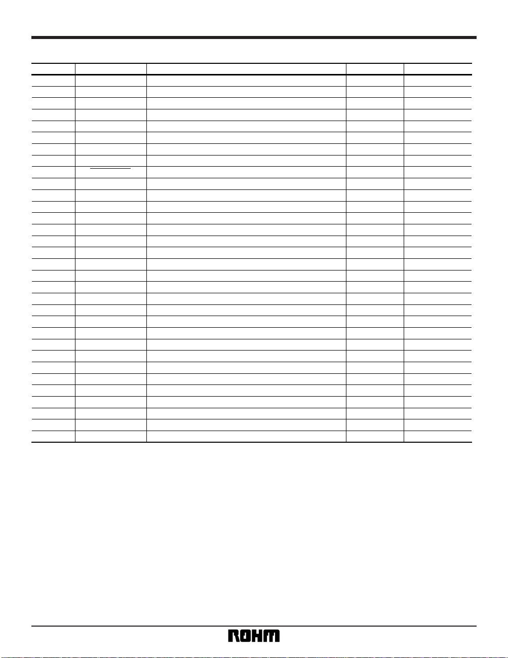
1 MODE 1
—
25kΩ
2 PRE OUT R 1.65
3 INV IN R 1.65 100kΩ
4 INV OUT R 1.65
5 MTX IN R 1.65 B
6 MTX OUT R 1.65
7 HPF IN R 1.65 100kΩ
8 OUT R 1.65
9 MIC MONO — C
10 MIX OUT 1.65
11 LPF INV IN — B
12 LPF INV OUT —
13 V
CC
3.3 —
14 BIAS 1.65
15 DET IN 1.65 2kΩ
16 DET OUT — 22kΩ
17 OUT L 1.65
18 HPF IN L 1.65 100kΩ
19 MTX OUT L 1.65
20 MTX IN L 1.65 B
21 INV OUT L 1.65
22 INV IN L 1.65 100kΩ
23 PRE OUT L 1.65
24 MODE 24 — 25kΩ
25 EXT IN L 1.65 75kΩ
26 BG 1.25 10kΩ
27 INT IN L 1.65 75kΩ
28 GND ——
29 VREG 2.5 C
30 INT IN R 1.65 75kΩ
31 RIPL 1.65 50kΩ
32 EXT IN R 1.65 75kΩ
EF (P - P)
EF (P - P)
EF (P - P)
C (P - P)
EF (P - P)
EF (P - P)
EF (P - P)
C (P - P)
EF (P - P)
EF (P - P)
EF (P - P)
Pin name FunctionPin No. Voltage (
V)
∗
EF: emitter follower, P-P: push pull, B: base, and C: collector.
Circuit
Mode control 1 input
Preamplifier output
Inverter input
Inverter output
Matrix amplifier input
Matrix amplifier output
High-pass filter input
Signal output
External microphone monaural decision signal output
Mix Output
Low-pass filter block inverter input
Low-pass filter block inverter output
V
CC
Bias voltage
Detector circuit input
Detector circuit output
Signal output
High-pass filter input
Matrix amplifier output
Matrix amplifier input
Inverter output
Inverter input
Preamplifier output
Mode control 24 input
External microphone input
For regulator ripple filter capacitor
Internal microphone input
GND
Regulator output
Internal microphone input
For bias ripple filter capacitor
External microphone input
All numerical values are standardized values.
•
Pin descriptions
Page 4

4
Video ICs BA7781K
•
Measurement circuit
21 3
4
5
6
7
8
24
23
22
21 20 19 18 17
16
15
14
13
11
10
9
25
27
28
29
30
31
32
EXT
INT
13dB
13dB
GND
REG
BIAS
INT
EXT
+
–
NOR
WND
NOR
WND
15dB
+
–
EXT
EXT
BIAS
V
CC
MIX
+
–
10dB
15dB
–
+
DET
0.1µ
10k 10.5k
0.1µ
0.1µ
1212
2200p
0.1µ
0.1
µ
0.1
µ
2200p
SW2
HPF IN
2.2µ
+
1M
0.1µ
0.1µ
200k
200k
10µ
+
10k
10.5k
1
2
MODE 24
SW1
MODE 1 HPF IN
L OUT
V
CC
INV (11) IN
R OUT
EXT IN
INT IN
INT IN
EXT IN
GND
0.1µ
10µ
0.1µ
30k
0.1µ
10µ
0.1µ
Lch
Rch
+
+
UNITS
RESISTOR: Ω
CAPACITOR: F
26
12
Fig. 1
Page 5

5
Video ICs BA7781K
•
Application example
12
EXT
INT
13dB
13dB
GND
REG
BIAS
INT
EXT
+
–
NOR
WND
NOR
WND
15dB
+
EXT
EXT
BIAS
V
CC
MIX
+
–
10dB
15dB
–
+
DET
0.1µ
10k 10.5k
100k
0.1µ
0.022µ
2200p
0.1µ
0.1µ
2200p
2.2µ
+
1M
100k
220k
150k
10µ
+
1µ
+
10k
10.5k
100k
A
B
L OUT
V
CC
MIC-MONO
R OUT
EXT IN
INT IN
INT IN
EXT IN
0.1µ
10µ
0.1µ
0.1µ
10µ
0.1µ
+
+
0.022µ
24k
15k
15k
A'B'
2200p
0.01µ
0.01µ
24k
0.022µ
0.022µ
GND
R ch
L ch
UNITS
RESISTOR: Ω
CAPACITOR: F
Additional components INT / EXT monitoring
INT / EXT
L OPEN
100k
29
1
2
3
4
5
24
23
22
21 20
19 18 17
16
13
12
11
10
9
26
27
28
30
31
32
67
25
15
8
14
100k
∗
1) When using the matrix circuit connect A-A' and B-B'.
∗
2) The pin 10 and 12 low-pass filter components are for fc = 150Hz, Gain = 0dB, 18dB / oct.
–
Fig. 2
Page 6

6
Video ICs BA7781K
•
Measurement circuit switch table (blank cells: no spesification)
SW1 SW2 MODE1 MODE24
11 H L
11
11
11
11
11
11
1 1 L L INT
1 1 H L INT
1 1 L L EXT
11
1 1 H Vth
1 1 Vth L
2 2 H L INV (11) , HPF
1 1 H L INV (11) , INT
11 H L
2 2 H L HPF, 16pin of Vth
INV, 16pin of Vth
INT, EXT
INT, EXT
EXT
INT
Signal input pin
Parameter
Current dissipation 1
Current dissipation 2
Preamplifier gain
Output amplifier gain
Distortion
Maximum output
Output noise voltage
Input switch separation (INT
→ EXT)
Interchannel separation
Internal microphone power supply voltage
Input switch control voltage
High-pass filter switching attenuation characteristic
High-pass filter control voltage
Conditions other than No. 1
∗
H and L are VCC and GND levels.
Measure the voltage range that maintains the mode for Vth.
•
Operation notes
(1) Automatic wind-noise rejection circuit
The MAX OUT (pin 10) signal passes through the
three-stage low-pass filter connected between pins 10
and 12, and the DC level of the low-frequency signal
component is detected. This DC voltage (pin 16 DC
voltage) automatically controls the on / off switching of
the high-pass filter. The components connected to pins
11 and 12 set the gain of a multiple-feedback-type twostage low-pass filter constructed around an inverting
amplifier, and by changing the gain of the circuit you
can adjust the detection sensitivity.
It is also possible to switch the high-pass filter manually
by applying a DC voltage to pin 16 (see Fig 2).
(2) Additional compornents for INT / EXT monitor use
An internal circuit sets pin 12 to roughly the bias potential in INT mode, and to GND for EXT mode. This
switches the external transistor on and off for INT and
EXT modes respectively. This can be used to indicate
whether the microphone amplifier is operating with the
INT or EXT input. In the case of a camcorder, this can
be used to display a massage such as “EXT MIC ON”
in the EVF.
Page 7

7
Video ICs BA7781K
•
Electrical characteristic curves
OUTPUT LEVEL: VROUT (dBV)
15PIN INPUT SIGNAL LEVEL: VDETIN (dBV)
VCC = 3.3V
Ta = 25°C
– 60
– 40
– 20
0
– 60 – 50 – 40 – 30 – 20 – 10
Input: 80Hz
NOR side output
6
→
8pin
HPF side output
7
→
8pin
Fig. 3 HPF switching characteristics
16PIN DETECT OUTPUT: VDETOUT (V)
15PIN INPUT SIGNAL LEVEL: VDETIN (dBV)
VCC = 3.3V
Ta = 25°C
0
0.5
1.0
1.5
2.0
2.5
– 60 – 50 – 40 – 30 – 20 – 10
Input: 80Hz
Fig. 4 Detector voltage characteristis
•
External dimensions (Units: mm)
0.15
0.4 ± 0.1
24
17
16
9
8
1
25
32
7.0 ± 0.2
9.0 ± 0.3
7.0 ± 0.2
9.0 ± 0.3
0.4
0.05
1.45 ± 0.1
0.15 ± 0.1
0.8
QFP32
 Loading...