

Page 1

1
Video ICs
VCR Hi-Fi audio signal REC / PB
amplifier
BA7746S / BA7746FS
The BA7746S and BA7746FS contains the recording and playback amplifiers required for Hi-Fi VCR signal processing. The recording system uses a constant-current amplifier with AGC to eliminate the need to adjust the recording
current, and ensure stable operation as the head wears. The IC also features REC MUTE and OVER REC functions.
The playback system has a high-gain preamplifier, a low- offset head switch, VCA, and an EP-gain amplifier.
In addition, all functions operate off a single 5V supply, and a H / L control system eliminates the need for special
power supplies for the recording and playback systems. The IC has low power consumpution, and comes in a compact 32-pin SSOP-A package that requires little area on the PCB. It will improve the reliability and performance of
your designs while reducing external component requirements.
•
Applications
VCRs
•
Features
1) The low-noise playback amplifier has a total gain of
79dB (Typ.). Designed for VHS-band operation with
low external parts count. It has two built-in circuits
for Hi-Fi VCR operation.
2) The circuit has been designed to suppress headswitching noise.
3) Built-in EP / SP gain switching function that boosts
the playback gain by 5dB.
4) Built-in VCA for easy playback output adjustment.
5) High-output recording amplifier for audio FM recording.
6) Constant-current drive povides stable recording
characteristics when the load (head impedance) is
fluctuating.
7) Built-in recording level AGC eliminates the need to
adjust recording current.
8) Built-in low-pass filter limits the input bandwidth of
the recording amplifier.
9) Built-in OVER REC recording current amplifier
function and REC MUTE function that stops recording output.
10) Low power consumption. Operates off a single 5V
power supply.
11) Record / playback switching can be done directly
via the system controller, and consumes littele
power.
12) Possible to construct a high-performance audio
system by pairing this chip with a Hi-Fi-audio signal
processing IC.
•
Absolute maximum ratings (Ta = 25°C)
Parameter
Symbol Limits Unit
V
CC 7.0 V
BA7746S
BA7746FS
Pd
1050
∗
1
mW
800
∗
2
mW
Topr – 10 ~ + 70
°C
Tstg – 55 ~ + 125 °C
∗
1 When mounted on a 90mm × 50mm × 1.6mm glass epoxy board, reduced by 10.5mW for each increase in Ta of 1°C over 25°C.
∗
2 When mounted on a 90mm × 50mm × 1.6mm glass epoxy board, reduced by 8mW for each increase in Ta of 1°C over 25°C.
Power supply voltage
Power
dissipation
Operating temperature
Storage temperature
Page 2
2
Video ICs BA7746S / BA7746FS
•
Recommended operating conditions (Ta = 25°C)
Parameter
Symbol Min. Typ. Max. Unit
V
CCS 4.5 5.0 5.5 V
Operating voltage
•
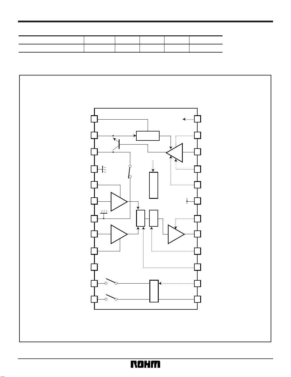
Block diagram
23
24
22
21
20
19
18
17
16
15
14
13
1
2
3
4
5
6
8
7
10
11
12
REC
VCA
PRE PRE
AGC
PB / REC
SW
EP
TC
P
P / R
ch1ch2
ch2ch1
RR
N.C.
REC AGC FILTER
REC CURRENT SENSE
REC OUT
MAIN GND
PRE AC – FB ch1
PRE IN ch1
PRE GND
PRE IN ch2
PRE AC – FB ch2
N.C.
REC + B ch2
REC + B ch1
REC / PB CTRL
REC NF
REC MIX IN
OVER REC CTRL
REC MUTE CTRL
V
CC
VCA CTRL
(PRE MUTE)
PRE OUT
HSWP IN
EP / SP CTRL
REC TC
V
CC REC + B
9
Page 3
3
Video ICs BA7746S / BA7746FS
•
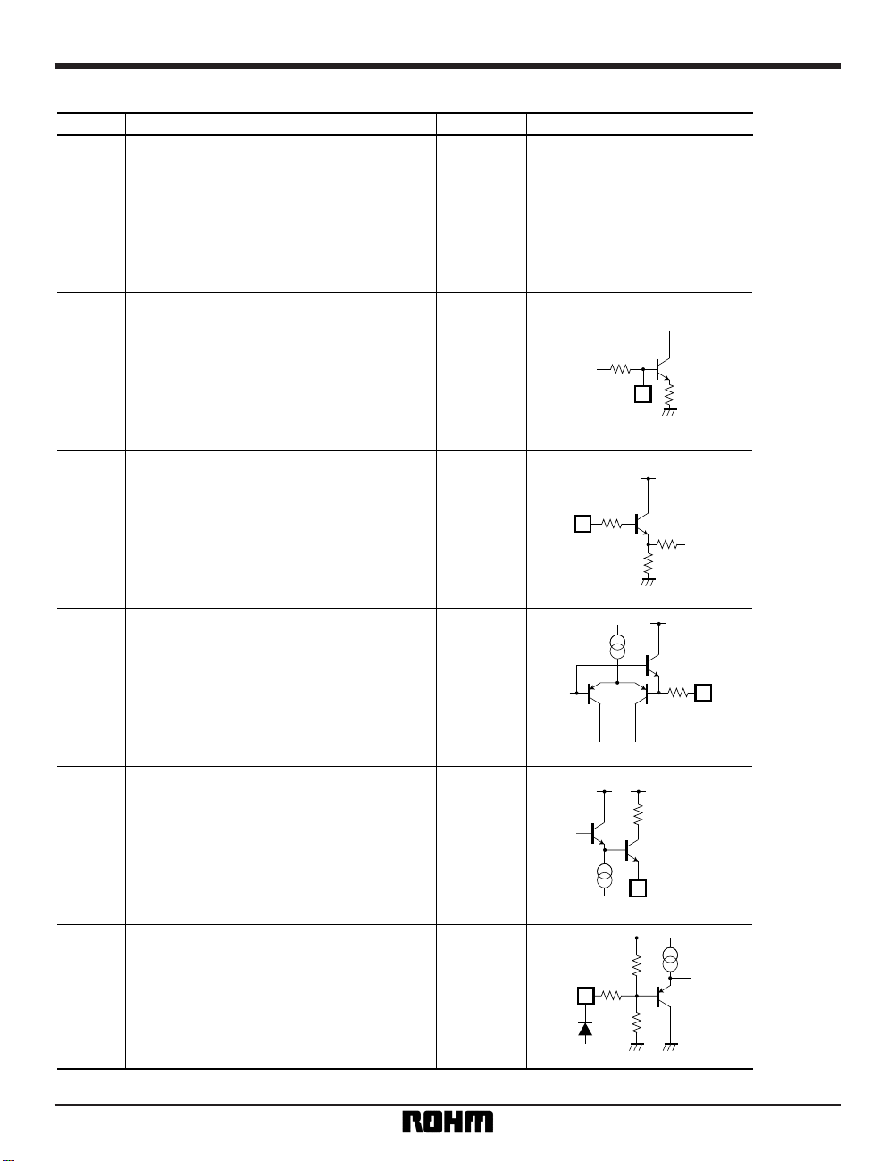
Pin descriptions
1
2
REC: 0.9V
PB: 0V
3—
4—
5
REC: 3.6V
PB: 1.9V
6
REC: 2.0V
PB: 2.0V
V
CC —
(RL: 1.8k
Ω)
Pin No. Circuit diagramPin name, function and remarks Voltage
〈V
CC REC + B〉
•
Power supply for REC + B.
•
Connect to VCC (pin 7).
〈REC TC〉
•
REC + B time constant.
•
Use to adjust the REC + B rise time using the C
value. The value of the built-in resistor is 20kΩ.
•
The effect of current spikes when recording is
started is reduced
〈HSWP IN〉
•
Pulse input for head switching.
•
ch1: H, ch2: L
〈EP / SP CTRL〉
•
EP / SP mode control.
•
In EP mode, the playback amplifier gain is set to
+ 5dB (Typ.).
•
EP: H, SP: L
•
Do not leave open circuit
〈PRE OUT〉
•
Playback amplifier output.
•
Open emitter output.
•
When there is a chance of oscillation due to
capacitive load, reduce the output current, or
connect a resistor in series (approx. 390Ω).
•
Avoid capacitive coupling with the playback input
〈VCA CTRL (PRE MUTE)〉
•
VCA control.
•
When the terminal is open (a C is required), the
playback amplifier gain is set to the Typ. value.
•
The PRE MUTE function is made possible by
connection of a mute H signal to this
through a diode
20k
REC
24k
EP SP
40k
MUTE H
580
30k
20k
Page 4
4
Video ICs BA7746S / BA7746FS
7VCC —
8—
9—
10
REC: 2.9V
PB: 2.9V
11
REC: 1.4V
PB: 0.5V
12 —
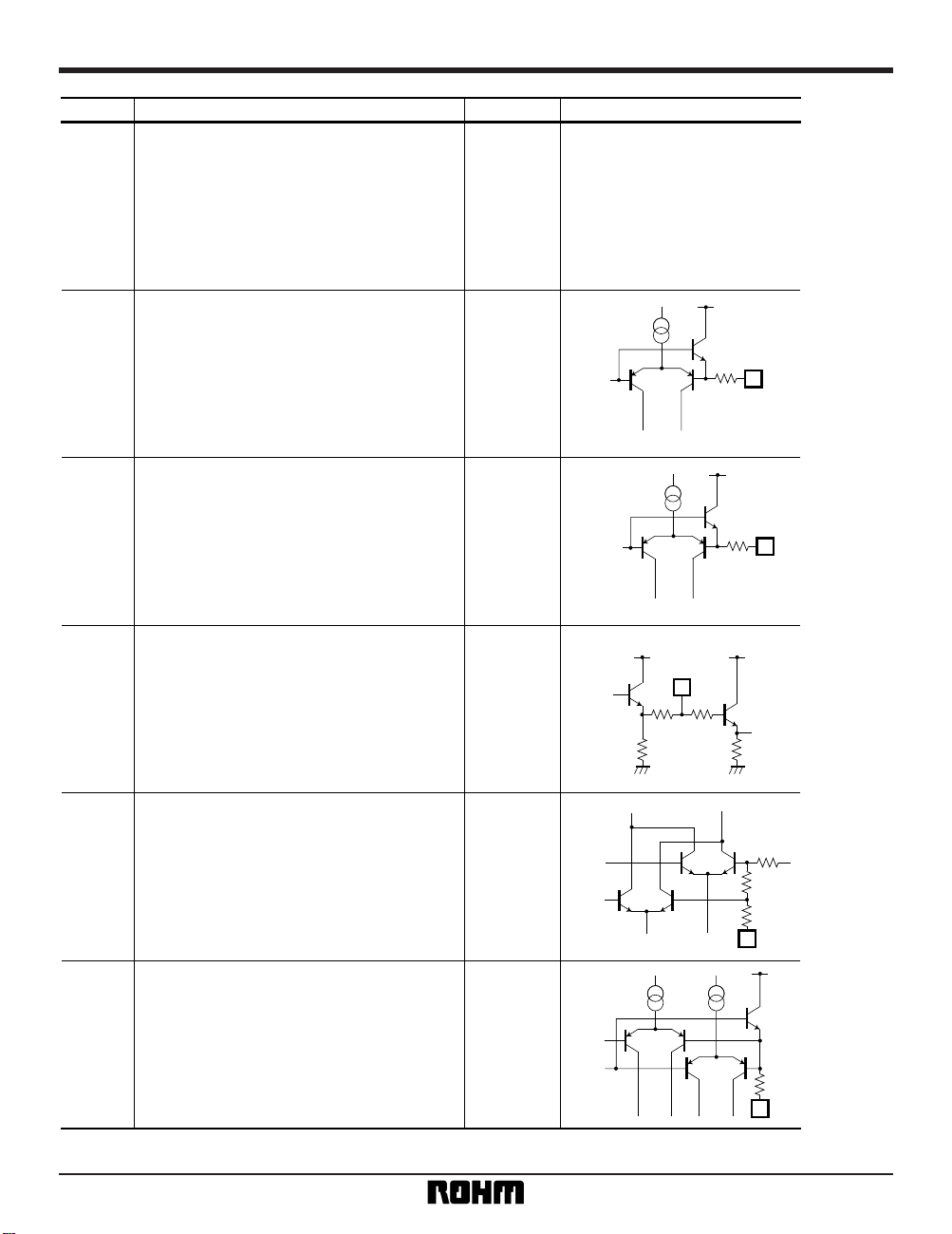
Pin No. Pin name, function and remarks Voltage Circuit diagram
〈V
CC〉
•
Power supply for anything other than REC + B.
〈REC MUTE CTRL〉
•
REC MUTE control.
•
In REC MUTE mode, the recording amplifier
output is stopped.
•
REC: L, REC MUTE: H.
•
Do not leave open circuit.
〈OVER REC CTRL〉
•
OVER REC control.
•
In OVER REC mode, the recording current is set
to + 2dB (Typ.).
•
Do not leave open circuit.
〈REC MIX IN〉
•
Recording amplifier input.
〈REC NF〉
•
Recording amplifier feedback.
•
Connect the GND of a decoupling capacitor to
main GND (pin 16) to improve common-mode
distortion.
〈REC / PB CTRL〉
•
REC / PB control pin.
•
Use of an RC circuit time constant to slow the rise
of the control signal reduces noise spikes during
switching.
•
Do not leave open circuit.
MUTE REC
30k
OVER NORMAL
30k
10k 10k
10.2k
240
1.04k
30k
Page 5

5
Video ICs BA7746S / BA7746FS
13
REC: 0V
PB: 0V
14
REC: 0.58V
PB: 0V
15
REC: 4.1V
PB: 0V
16 GND —
17
REC: 0V
PB: 0.8V
18
REC: 0V
PB: 0.7V
Pin No. Pin name, function and remarks Voltage Circuit diagram
〈REC AGC FILTER〉
•
REC AGC filter.
•
The attack characteristics of the recording amplifier
can be adjusted using the CR circuit.
•
Reduce the CR circuit GND-side impedance to
improve the common-mode distortion.
〈REC CURRENT SENSE〉
•
Terminal for monitoring the recording current.
•
Open emitter output.
•
The REC AGC output current can be adjusted with
the R value.
e.g. 12Ω...48.2mA
P-P, 15Ω...38.6mAP-P
〈REC OUT〉
•
Recording amplifier output and head switch.
•
Open collector output.
•
The head switch turns on and off in accordance with
the REC / PB control signal
〈MAIN GND〉
•
Earth for circuits other than the preamplifier.
•
Reference potential for the IC
〈PRE AC-FB ch1〉
•
AC feedback terminal for the playback amplifier
(ch1).
•
The high-frequency characteristics of the playback
amplifier can be adjusted with the R value
〈PRE IN ch1〉
•
Input terminal for the playback amplifier (ch1).
•
The low-frequency cutoff characteristics can be
adjusted with the value of the input coupling
capacitor.
•
The frequency characteristics can be adjusted so
that it is flat with the L value of the rotary
transformer, and the external capacitor C (100pF
etc.).
2k
2k
14
15
17
18
4k
13k
Page 6

6
Video ICs BA7746S / BA7746FS
19 GND
20
REC: 0V
PB: 0.7V
21
REC: 0V
PB: 0.8V
22 —
—
—
23
REC: 4.1V
PB: 0V
24
REC: 4.1V
PB: 0V
Pin No. Pin name, function and remarks Voltage Circuit diagram
〈PRE GND〉
•
GND for the HEAD AMP.
•
Use this terminal for the pin 17 to pin 21 GND
connections to improve the noise characteristics.
•
Connect this pin to the main GND (pin 16).
〈PRE IN ch2〉
•
Inputl for the playback amplifier (ch2).
The low-frequency cutoff characteristics can be
adjusted with the value of the input coupling
capacitor.
•
The frequency characteristics can be adjusted so
that it is flat with the L value of the rotary
transformer, and the external capacitor C (100pF
etc.).
〈PRE AC-FB ch2〉
•
AC feedback for the playback amplifier (ch2).
•
The high-frequency characteristics of the playback
amplifier can be adjusted with the R value.
〈N.C.〉
•
Unused.
•
Connect to 〈MAIN GND〉 to improve the
interchannel matching.
〈REC + B ch2〉
•
REC + B (ch2).
•
Open emitter output circuit.
•
Turns on and off in accordance with the REC / PB
control signal.
〈REC + B ch1〉
•
REC + B (ch1).
•
Open emitter output circuit.
•
Turns on and off in accordance with the REC / PB
control signal.
∗
The values given above are design values, they are not ratings and are not guaranteed.
4k
13k
21
20
Page 7

7
Video ICs BA7746S / BA7746FS
•
Electrical characteristics
Recording mode (pin 12→ "H") (unless otherwise noted, Ta = 25°C, V
CC = 5.0V, and f = 1.7MHz)
Parameter Symbol Min. Typ. Max. Unit Conditions
Iq
(REC)
—6690mA
I
OAR
44.2 48.2 52.2 mA
P-P
∆I
OAR
10 13 — dB
CMD
04
— – 50 – 40 dB
CMD
09
— – 55 – 40 dB
V
9L
0.0 — 2.2 V
V
9H
3.5 — V
CC
V
I
OR.OV
dB
V
8L
0.0 — 2.2 V
V
8H
3.5 — V
CC
V
I
OR.MU
— – 50 – 40 dB
10pin 93.0dBµIN, 14pin OUT
∆AGC
<
0.8dB, 14pin OUT
14pin OUT (0.4MHz - 1.3MHz)
14pin OUT (0.9MHz - 1.3MHz)
10pin 93.0dBµIN, 8pin: “H”
10pin 93.0dBµIN, 9pin: “H”2.4
10pin MIXIN
∗
,
10pin MIXIN
∗
,
1.91.4
9pin DC, When NORMAL REC
9pin DC, When OVER REC
8pin DC, When MUTE OFF
8pin DC, When MUTE ON
∗
f = 1.3MHz (87.0dBµ) + 1.7MHz (95.0dBµ) (MIX)
No signal, pin 1 + pin 7, inflow current
Quiescent current
Output current AGC level
Output current AGC level
Cross modulation distortion
0.4MHz component
Cross modulation distortion
0.9MHz component
OVER REC holding voltage
OVER REC holding voltage
Current emphasis OVER
REC MUTE holding voltage
REC MUTE holding voltage
Mute attenuation
Playback mode (pin 12→ "L") (unless otherwise noted, Ta = 25°C, VCC = 5.0V, and f = 1.5MHz)
Parameter Symbol Min. Typ. Max. Unit Conditions
—1931mA
G
VP1
75 79 83 dB
G
VP2
75 79 83 dB
– 2.0 0 dB
CT
1→2
— – 45 – 35 dB
CT
2→1
— – 45 – 35 dB
f
P1
0 – 2.4 – 5 dB
f
P2
0 – 2.4 – 5 dB
– ∆G
VCA
— – 50 – 35 dB
—dB
V
OMP
2.0 2.6 — V
P-P
V
NP1
— 0.4 1.0 µV
rms
V
NP2
— 0.4 1.0 µV
rms
∆G
VP
+
∆G
VCA
18pin, 20pin, 20.5dBµ,
18pin 31.0dBµ, 20pin 0 IN,
18pin 0, 20pin 31.0dBµIN,
f = 2.2MHz / 1.0MHz, ∆5pin OUT
f = 2.2MHz / 1.0MHz, ∆5pin OUT
6pin 3.2V, ∆5pin OUT
6pin 0.8V, ∆5pin OUT
Pin 18 and 20 IN, pin 5 OUT 3rd-harmonic
distortion, when-30dB.
Input conversion for pin 18: 0.01µ
F +
10Ω at GND Pin 3: “H”, pin 5 OUT.
Input conversion for pin 20: 0.01µF +
10Ω at GND Pin 3: “L”, pin 5 OUT.
Iq
〈PB〉
3pin: “H”
3pin: “L”
3pin: “H”→
“L”,
∆5pin OUT
18pin, 20.5dBµIN, 5pin OUT,
20pin, 20.5dBµIN, 5pin OUT,
∆5pin OUT
3pin: “L”→
“H”,
∆5pin OUT
18pin 20.5dBµIN, 3pin: “H”
20pin 20.5dBµ IN, 3pin: “L”
2.0
46
Supply current
Voltage gain CH1
Voltage gain CH2
Voltage gain differential
CH1 to CH2 crosstalk
CH2 to CH1 crosstalk
CH1 frequency characteristic
CH2 frequency characteristic
Gain adjustment headroom
Gain adjustment headroom
Maximum output voltage
CH1 input conversion noise
CH2 input conversion noise
Inflow current to pin 7 when no signal.
Page 8

8
Video ICs BA7746S / BA7746FS
•
Electrical characteristics
Playback mode (pin 12→ "L") (unless otherwise noted, Ta = 25°C, V
CC = 5.0V, and f = 1.5MHz)
Parameter Symbol Min. Typ. Max. Unit Conditions
V
HS2
0.0 — 2.2 V
V
HS1
2.8 — V
CC
V
∆V
ODC
– 20 0 mV
0.0 — 1.0 V
3.5 — V
CC
V
R
SWP
— 510Ω
0.0 — 2.2 V
3.5 — V
CC
V
G
VP.EP
4.0 5.0 6.0 dB
18, 20pin 0 IN,
3pin “H”→
“L”
∆5pin OUT
5pin OUT
V
12L
V
12H
V
4L
V
4H
18, 20pin 20.5dBµIN, 4pin: “H”,
20
Head switching voltage
Head switching voltage
Output DC offset
PB holding voltage
REC holding voltage
Head switch ON resistance
SP holding voltage
EP holding voltage
Gain emphasis EP
Pin 3 DC when ch2 operating
Pin 3 DC when ch1 operating
Pin 12 DC for PB mode
Pin 12 DC for REC mode
Pin 15 ON resistance
Pin 4 DC for SP mode
Pin 4 DC for EP mode
•
Measurement circuit
REC
VCA
PRE PRE
EP
PB / REC
P / R
SW
RR
ch1 ch2
ch2 ch1
TC
12µ 12µ
24
23 22 21 20 19 18 17 16 15 14 13
12
1110987654321
N.C.
560 560
0.1
µ
0.1µ
0.01
µ
0.01
µ
10 10
100p 100p
1k
1k
PRE IN ch2
PRE IN ch1
P
680
220p
12
AGC
0.22µ
68k
0.1µ
0.01µ
0.01µ
100µ
100µ
PR / REC
CTRL
5V
20k
REC MIX IN
OVER REC
CTRL
REC MUTE
CTRL
EP / SP CTRL
PRE OUT
HSWP IN
7pin SHORT
390
1.8k
0.01µ
0.047µ
220k
0.1µ
CURRENT
SENSE
Fig. 1
Page 9

9
Video ICs BA7746S / BA7746FS
•
Control mode tables
(1) REC / PB control
Switch between REC and PB using pin 12.
REC / PB
H REC ON OFF ON OFF
L PB OFF ON OFF ON
REC + B SWREC AMP PRE AMP HEAD SW (P)
Mode
Control pin Function
(2) OVER REC control
Control for OVER REC (current emphasis) is done using pin 9.
When in OVER REC mode, the gain setting is recording
amplifier AGC level + 1.9dB.
H
L—
60.0mAP-P
48.2mAP-P
OVER REC
OVER REC
Mode
Function
REC AGC Level
Control pin
(3) REC MUTE control
Control for REC MUTE when recording is done using pin 8.
REC MUTE REC AMP
H REC MUTE OFF
L—ON
Mode
Control pin Function
(4) EP / SP control
EP / SP control during playback is done using pin 4. When
EP is selected, the gain of the playback amplifier is increased
by 5dB over its normal setting.
EP / SP
H EP Typ. + 5dB
L SP Typ.
Mode
Function
PRE AMP gain
Control pin
Page 10

10
Video ICs BA7746S / BA7746FS
•
Application example
REC
VCA
PRE PRE
EP PB / REC
P / R
SW
RR
ch1 ch2
ch2 ch1
TC
24 23 22 21 20 19 18 17 16 15 14 13
121110987654321
N. C.
560 560
0.1µ 0.1µ
0.01µ 0.01µ
560 560
100p 100p
P
680
220p
12
AGC
0.22µ
68k
0.1µ
0.01µ
0.01µ
100µ
100µ
PB / REC CTRL
5V
REC MIX IN
OVER REC CTRL
REC MUTE CTRL
EP / SP CTRL
PRE OUT
HSWP IN
7pin SHORT
390
1.8k
0.01µ
0.047µ
AUDIO HEAD
220k
0.1µ
CURRENT
SENSE
Fig. 2
Page 11

11
Video ICs BA7746S / BA7746FS
•
Operation notes
(1) preamplifier
The preamplifier in this IC is a high-gain amplifier for
FM audio. This amplifier has been carefully designed
for stability. However, the design of the PCB greatly
effects the stability of the preamplifier. A list of general
precautions are given below. Take note when designing the PCB.
1)The oscillation margin is reduced when the input
and output patterns are physically close.
The input and output wiring should not come out of
the same side of tha IC.
Good example
Bad example
2)The GND pattern should be connected at one point
to the main IC GND (pin 16). In addition, the preamplifier input-side GND and output-side GND should
be as close as possible to the main IC GND.
Good example
Bad example
3)A large GND pattern under the IC has a shielding
effect, and reduced the chance of picking up external noise.
4)When the preamplifier is connected to a capacitive
load such as shilded wire, or when the output current is large, the output may oscillate. In this case,
connect a resistor to the preamplifier output (approx.
390Ω).
ICInput Output
PRE
GND
MAINIC
RL
GND GND
Output
Output
Input
390
REC
PRE
HEAD AMP
660mV
P-P
BA7746S / FS
270mV
P-P
BH780XK series
REC
LPF
REC
LPF
MOD
MOD
FM
BPFDEMOD
Connection example for BA7746S / BA7746FS and BH780XK series.
Hi-Fi AUDIO
IC
Output
Input
PRE
GND
MAINIC
R
L
GND GND
Output
OutputInput
Page 12

12
Video ICs BA7746S / BA7746FS
(2) REC amplifier
The REC amplifier in this IC is for FM audio. Take note
of the following points in order to maintain its commonmode distortion characteristics.
1)Connect the REC AGC FILTER (pin 13) and CUR-
RENT SENSE (pin 14) to the main GND of the IC (pin
16) using leads that are as short as possible.
2)REC NF (pin 11) should be as close to the main IC
GND as possible.
3)If you connect a resistor to pin 23 or between pins
24 and 15 to monitor the recording current, the resulting voltage drop may cause the IC to function incorrectly. Use the current sense pin (pin 14) to monitor the
recording current.
•
External dimensions (Units: mm)
SSOP-A24
SDIP24
0.51Min.
6.5 ± 0.3
0.3 ± 0.1
7.62
3.4 ± 0.2
22.9 ± 0.3
0.5 ± 0.11.778
13
12
24
1
3.95 ± 0.3
0° ~ 15°
BA7746S BA7746FS
0.15
0.3Min.
7.8 ± 0.3
5.4 ± 0.2
1.8 ± 0.1
0.11
1
24
0.36 ± 0.1
10.0 ± 0.2
12
13
0.8
0.15 ± 0.1
 Loading...