

Page 1

1
Multimedia ICs
Analog compander with vocal fader
for KARAOKE
BA7726AS / BA7726AFS
The BA7726AS and BA7726AFS are analog companders for karaoke echo systems and have internal logarithmic
compression and expansion circuits, a stereo line mixer amplifier, vocal fader function, vocal detection function,
microphone ALC, microphone ON / OFF switch, and output switch. When used together with the BU9252 8-bit digital
delay, these ICs form a high-grade karaoke echo system with minimum components.
•
Features
1) Internal stereo line mixer amplifier, allowing selection of through output, left output, or right output.
2) Internal vocal elimination function, suitable for vocal
faders and left and right output.
3) Echo level and loop ratio are DC-adjustable with the
internal electronic volume control (EVR).
4) Internal microphone ON / OFF switch.
5) Vocal detection.
6) Internal microphone ALC function.
7) Internal anti-popping circuit.
•
Applications
Portable CD stereos with karaoke functions, VCRs, mini component stereo systems, LD players
•
Absolute maximum ratings (Ta = 25°C)
Parameter Symbol Limits Unit
Power supply voltage V
CC 14 V
Power dissipation
BA7726AS
mW
BA7726AFS
Operating temperature Topr °C
Storage temperature Tstg °C
1250
∗
1
850
∗
2
Pd
– 10 ~ + 70
– 55 ~ + 125
∗
1 Reduced by 12.5mW for each increase in Ta of 1°C over 25°C.
∗
2 Reduced by 8.5mW for each increase in Ta of 1°C over 25°C.
•
Recommended operating conditions (Ta = 25°C)
Parameter Symbol Min. Typ. Max. Unit
Power supply voltage V
CC 4.5 9.0 12.0 V
Page 2

2
Multimedia ICs BA7726AS / BA7726AFS
•
Block diagram
123456789
32 31 30 29 28 27 26 25 24 23 22 21 20 19 18 17
10 11 12 13 14 15 16
OUTSW
VOCAL
FADER
SW
VOCAL
DET
ALC
VR
–
+
EXPAND
COMPRESS
–
+
–
+
VR
VR
BIAS
GND
VCC
LINE OUT R
LINE OUT L
L / VF / R CTRL
MUTE CTRL
LINE IN R
LINE IN L
VF LPF1
VF LPF2
LOOP GAIN CTRL
EXP DET
EXP DET CT
EXP BF IN
DLY BF OUT
L / ST / R CTRL
NO / VC CTRL
VO DET
VO DET LEVEL
ALC DET LEVEL
ALC DET
MIC AMP IN
MIC AMP NF
CMP DET
CMP DET CT
CMP OUT
CMP BF NF IN
CMP BF OUT
DLY BF NF IN
VF LPF3
ECHO LEVEL CTRL
Page 3
3
Multimedia ICs BA7726AS / BA7726AFS
•
Pin descriptions
Note: Pin type EF: emitter follower, P-P: push-pull, B: base
For pins marked with an asterisk (
∗
), refer to Input and output equivalent circuit.
Pin No. Pin name Function Voltage Pin type
2, 1 LINE OUT L / R Line output (L, R) 4.5V EF (P - P)
3 L / VF / R CTRL
Line output switching (LEFT / VOCAL FADER / RIGHT)
2.5V
4 MUTE CTRL Line mute control input —
6, 5 LINE IN L / R Line input (L, R) 4.5V 100kΩ
7 VF LPF1 Vocal fader mode LPF capacitor 4.5V 23.5kΩ
8 VF LPF2 Vocal fader mode LPF capacitor 4.5V 70.5kΩ
9 VF LPF3
Vocal fader mode LPF capacitor
4.5V EF (NPN), 15kΩ
10 GND Ground 0.0V —
11 ECHO LEVEL CTRL Microphone off (ground to 0.1Vcc) / echo level adjustment (0.2Vcc to Vcc) —
12 LOOP GAIN CTRL Loop attenuation ratio setting —
13 EXP DET Expand detection wave 4.5V 50kΩ
14 EXP DET CT
Expand attack / recovery time setting
Attack R = 5.6kΩ , recovery R = 85.6kΩ
—
15 EXP BF IN BF input 4.5V B (NPN)
16 DLY BF OUT LPF BF output (EXP) 4.5V EF (NPN)
17 DLY BF NF IN LPF BF negative feedback input (EXP) 4.5V B (NPN)
18 CMP BF OUT LPF BF output (CMP) 4.5V EF (P - P)
19 CMP BF NF IN LPF BF negative feedback input (CMP) 4.5V B (NPN)
20 CMP OUT Compression output 4.5V EF (NPN)
21 CMP DET CT
Compression attack / recover time setting
Attack R = 5.6kΩ, recovery R = 85.6kΩ
—
22 CMP DET Compression detection wave 4.5V 60kΩ
23 V
CC
V
CC
9.0V —
24 BIAS Bias and capacitor for ripple rejection 4.5V 23.5kΩ
25 MIC AMP NF Microphone amplifier negative feedback 4.5V 2kΩ
26 MIC AMP IN Microphone amplifier input 4.5V 100kΩ
27 ALC DET ALC attack / recovery time setting — 220Ω
28 ALC DET LEVEL ALC level setting — B (PNP)
29 VO DET LEVEL Microphone amplifier input detection level setting — B (PNP)
30 VO DET Microphone amplifier input detection attack / recover time setting — 1kΩ
31 NO / VC CTRL Line output switching (NORMAL / VOCAL CUT) —
32 L / ST / R CTRL Line output switching (LEFT / STEREO / RIGHT) 2.5V
—
—
All figures are designed values based on the measurement circuit in Fig. 1 (where Vcc = 9.0V), and are not guaranteed standards.
∗
∗
∗
∗
∗
∗
Page 4
4
Multimedia ICs BA7726AS / BA7726AFS
•
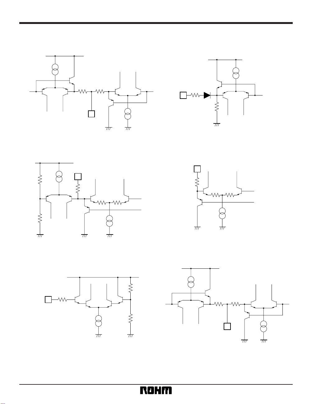
Input / output circuits
∗ All figures are designed values, and are not guaranteed standards.
VCC
3.3V
1.7V
3
VCC
85k
15k
11
39k
31
VCC
49.5k
33k
VCC
3.3V
1.7V
39k
0.6 × V
CC
0.8 × VCC
0.6 × VCC
0.8 × VCC
12
32
2.5V
150k
4
39k
39k 39k
39k 39k
39k
L / VF / R CTRL MUTE CTRL
LOOP GAIN CTRLECHO LEVEL CTRL
NO / VC CTRL L / ST / R CTRL
VCC
Page 5

5
Multimedia ICs BA7726AS / BA7726AFS
•
Electrical characteristics (unless otherwise noted, Ta = 25°C, Vcc = 9.0V)
Parameter Symbol Min. Typ. Max. Unit Conditions
Supply current I
CC 5.5 8.4 12.7 mA No input
Line through output level V
OLL – 9.0 – 8.0 – 7.0 dBV VIN = – 20.0dBV
Line through output distortion THD
LL — 0.026 0.2 %
Line through max. output level V
OMLL + 7.8 + 10.0 — dBV
Line through noise level V
ONLL — – 100 – 85 dBV
MIC OFF (V
ECHO = 0.1 × VCC)
Interchannel crosstalk CT
LL — – 85 — dBV
MIC OFF (V
ECHO = 0.1 × VCC)
Mute level MT — – 100 – 85 dBV
MUTE (V
MUTE = H)
MIC OFF (V
ECHO = 0.1 × VCC)
Through mode output level V
OLLV – 1.0 0.0 + 1.0 dBV VIN = – 12dBV
V
OLL1 – 1.0 0.0 + 1.0 dB
V
OLL2 —–35–28 dB
Microphone through output level
VOML – 9.9 – 8.4 – 6.9 dBV VIN = – 38dBV
Microphone through
equivalent input noise
V
ONML — – 117 – 102 dBV
Microphone input crosstalk CT
ML — – 92 – 77 dBV
MIC OFF (V
ECHO = 0.1 × VCC)
ALC level V
OAML + 5.1 + 6.6 + 8.1 dBV V28 = 2.9V
Compress output level V
OMC – 5.5 – 3.5 – 1.5 dBV VIN = – 38dBV
Compress characteristics CMP — + 5.2 — dB
V
IN = – 43dBV → – 33dBV
Output level differential
Expand output level V
ODL – 9.4 – 7.4 — dBV VIN = – 4dBV
Expand characteristics EXP — + 19.4 — dB
Echo EVR attenuation ratio — – 50 – 40 dB
Loop output level V
ODC – 4.4 – 2.4 — dBV VIN = – 4dBV
Loop EVR attenuation ratio — – 29 — dB
〈LINE THROUGH〉 INPUT : LINE IN, OUTPUT : LINE OUT
〈VOCAL CUT MODE〉 INPUT : LINE IN, OUTPUT : LINE OUT
〈MIC THROUGH〉 INPUT : MIC AMP IN, OUTPUT : LINE OUT
〈COMPRESS〉 INPUT : MIC AMP IN, OUTPUT : CMP BF OUT
〈EXPAND〉 INPUT : DLY BF IN, OUTPUT : LINE OUT
〈Loop〉 INPUT : DLY BF IN, OUTPUT : CMP BF OUT
∆V
ODC
∆VODL
LOOP GAIN = Min. (VLOOP = 0.2 × VCC)
V
IN = – 4dBV and when VIN = Vodc
ECHO LEVEL = Min. (V
ECHO = 0.2 × VCC)
V
IN = – 4dBV and when VIN = Vodl
V
IN = – 9dBV → + 1dBV, Output level differential
(V
LSTR = H, VLVFR = OPEN, VNOVC = OPEN)
V
IN = – 12dBV (dual ch.in.),VOCAL FADER
(V
LSTR = H, VLVFR = OPEN, VNOVC = OPEN)
V
IN = – 12dBV (single ch. in.),VOCAL FADER
MIC OFF (V
ECHO = 0.1 × VCC)
Vocal suppression ratio 1
Vocal suppression ratio 2
∗
1 Unless otherwise noted, mode settings are as follows.
∗
2 All parameters conform to the Measurement circuit diagram.
MUTE (V
MUTE = GND), STEREO (VNOVC = GND, VLSTR = OPEN, VLVFR = OPEN)
ECHO LEVEL = Max. (V
ECHO = VCC), LOOP GAIN = Max. (VLOOP = VCC)
Signal frequency : 1kHz,
∗
1 : B.W. = 0.4 ~ 30kHz, ∗2 : DIN AUDIO
VIN = – 20.0dBV
∗
1
No input, Rg = 1kΩ
∗
2
V
IN – 12dBV, Rg = 1kΩ
∗
2
V
IN = – 12dBV, Rg = 1kΩ
∗
2
THD = 1%
∗
1
Rg = 1kΩ
∗
2
V
IN = – 30dBV
∗
2
Page 6

6
Multimedia ICs BA7726AS / BA7726AFS
Parameter Symbol Min. Typ. Max. Unit Conditions
[ Control holding voltage ]
〈MUTE CTRL (4pin)〉
Mute holding voltage (4pin) VMUTE – L GND — 0.5 V
V
MUTE – H 4.5 — 5.0 V
Normal mode holding voltage V
NOVC – L GND — 0.3 × VCC V
V
NOVC – H 0.5 × VCC —VCC V
Left mode holding voltage V
LSTR – L GND — 0.5 V
Stereo mode holding voltage V
LSTR – M 2.2 — 2.8 V
Right mode holding voltage V
LSTR – H 4.5 — 5.0 V
Left mode holding voltage V
LVFR – L GND — 0.5 V
V
LVFR – M 2.2 — 2.8 V
Right mode holding voltage V
LVFR – H 4.5 — 5.0 V
V
ECHO – L GND — 0.1 × VCC V
V
ECHO – H 0.2 × VCC —VCC V
〈NO / VC CTRL (31pin)〉
VOCAL CUT mode holding voltage
〈L / ST / R CTRL (32pin)〉
〈
L / VF / R CTRL (3pin)〉
VOCAL FADER mode holding voltage
〈ECHO LEVEL CTRL (11pin)〉
MIC OFF holding voltage
MIC ON holding voltage
Mute holding voltage (4pin)
Page 7

7
Multimedia ICs BA7726AS / BA7726AFS
123456789
32 31 30 29 28 27 26 25 24 23 22 21 20 19 18 17
10 11 12 13 14 15 16
OUTSW
VOCAL
FADER
SW
VOCAL
DET
ALC
–
+
–
+
VLVFR
VMUTE
VECHO
VLSTR
VNOVC
V
CC 9V
2.2µ
4700p
10k
+
2.2µ
4700p
+
10k
1k 1k
0.1µ
0.1µ
0.015µ
0.068µ
0.1µ+0.47µ
100k
33µ
1k
+
6.8k
3.3k
+
2.2M
47µ
1k
0.1µ
+1µ+
22µ
A
+
0.1µ
0.47µ
+
100µ
5600p
18k
47k
3900p
18k
39k
220p
47k
3900p
5600p
18k
1µ
1µ
+
+
18k
10k
1k
220p
39k
COMPRESS
EXPAND
VLOOP
8.2k
VR
VR
VR
LINE OUT R
LINE OUT L
LINE IN R
LINE IN L
MIC AMP IN
CMP BF OUT
DLY BF IN
–
+
Fig. 1
•
Measurement circuit
Page 8

8
Multimedia ICs BA7726AS / BA7726AFS
•
Circuit operation
(1) MUTE CTRL (pin 4)
• Controls line muting.
2) L / ST / R CTRL (pin 32)
• Controls LINE OUT output in the NORMAL mode.
(2) OUTPUT CTRL (pins 3, 31, 32)
• LINE OUT output is controlled with pins 3, 31 and 32.
(Microphone mixing is controlled with pin 11.)
1) NO / VC CTRL (pin 31)
• Used to select the NORMAL and VOCAL CUT modes.
LH
MUTE MUTE
VMUTE (4pin)
LH
NORMAL
NORMAL : Normal output mode. Controlled by pin 32.
VOCAL CUT : Used to erase or attenuate vocals in
multiplexed karaoke recordings and
normal stereo music recordings.
Controlled by pin3.
VOCAL CUT
V
NOVC (31pin)
VLSTR (32pin)
L M (OPEN) H
LEFT STEREO RIGHT
RIGHT : LINE IN R input is output to LINE OUT L / R.
STEREO : LINE IN L / R input is output to LINE OUT L / R without modification
LEFT : LINE IN L input is output to LINE OUT L / R.
3) L / VF / R CTRL (pin 3)
• Controls LINE OUT output in the VOCAL CUT mode.
RIGHT : For recordings in which the right channel is karaoke
and the left channel is for vocals (with karaoke).
LEFT : For recordings in which the left channel is karaoke
and the right channel is for vocals (with karaoke).
VLVFR (3pin)
L M (OPEN) H
LEFT RIGHT
VOCAL FADER : Attenuates the vocals from normal stereo recordings.
VOCAL FADER
∗ When Vnovc = L, VLVFR = DON 'T CARE
When Vnovc = H, V
LSTR = DON 'T CARE
(3) ECHO LEVEL CTRL and MIC ON / OFF SW (pin 11)
• Between Vcc and 0.2 × Vcc: Controls echo signal
mixing ratio
Between Vcc and GND : Turns microphone input
sound (pin 26) to LINE OUT on and off
V
CC
~ 0.2 × V
CC
0.1 × V
CC
~ GND
V
ECHO
(11pin)
MIC ON and ECHO LEVEL CTRL MIC OFF
– 100
0
– 50
0
0.5 1.0
VECHO (11pin) P.P ratio : VECHO / VCC
MIC AMP IN ~ LINE OUT
(VIN = – 38dBV, f = 1kHz)
DLY BF IN ~ LINE OUT
(V
IN = – 4dBV, f = 1kHz)
LINE OUT Attenuation. : ATT (dB)
Fig. 2 LINE OUTattenuation ratio vs. Vecho (11pin)
partial pressure ratio
∗
These figures are for standard samples and
are not guaranteed standards.
(4) LOOP GAIN CTRL (pin 12)
• Adjusts the loop gain (pins 17 and 18).
0
0
0.5 1.0
V
CC = 9.0V
–50
–25
VLOOP (12pin) P.P ratio : VECHO / VCC
DLY BF IN
~
CMP BF OUT
(V
IN = – 4dBV, f = 1kHz)
CMP BF OUT Attenuation. : ATT (dB)
Fig. 3 CMP BF OUT attenuation ratio vs. Vloop
(pin 12) partial pressure ratio
∗
These figures are for standard samples and
are not guaranteed standards.
Page 9

9
Multimedia ICs BA7726AS / BA7726AFS
(5) LPF
• Use the internal operational amplifier and an
attached capacitor and resistor to configure a tertiary
LPF for anti-aliasing and smoothing.
Cutoff frequency
LPF constant
Pass band gain
R
1 R2 R3 C1 C2 C3
2kHz 22kΩ 56kΩ 47kΩ 6800pF 4700pF 270pF 0.6dB
3kHz 18kΩ 47kΩ 39kΩ 5600pF 3900pF 220pF 0.7dB
4kHz 15kΩ 39kΩ 33kΩ 4700pF 3300pF 180pF 0.8dB
LPF constant examples (V
CC
= 9.0V)
∗
CMP OUT (pin 20) output is positively correlated with Vcc. When Vcc is a voltage other than 9.0V, set the pass band gain so that maximum CMP side LPF output
(input to BU9252) is 5Vp-p. Make sure that the EXP side LPF constant does not exceed the load drive capability (minimum = 0.3mA, typical 0.5mA).
20 19 18 17
16
–
+
–
+
R1
R2
C3
R1
R3
C2
C1
C3
R3
R2
R1
C2
C1
R1
TO BU9252
FROM BU9252
Fig. 4 LPF
(6) Vocal fader function
• After the synchronous component of the left and
right channels is eliminated, LPF output is added to
the signal, which is then output (see figure below).
The vocal component is difficult to remove from certain types of sources.
56789
LINELINE
C2
C1
LPF
+
–
IN LIN R
TO OUTSW
Fig. 5 Vocal fader block
LPF constant examples
Cutoff frequency
LPF constant
C
1 C2
100Hz 0.022µF 0.1µF
150Hz 0.015µF 0.068µF
200Hz 0.01µF 0.047µF
∗
C1 and C2 are only necessary when using the vocal fader function.
(7) ALC level
• When Vcc is 9.0V, ALC level can be set roughly
between -4dBV and +9dBV, and is determined by the
voltage impressed on pin 28 (V
28, set with resistive
division between Vcc and the ground). ALC level is
calculated with the following equation, although slight
error occurs as V
28 approaches VCC.
0
0
V
CC = 9.0V
510
Set within this range
+ 10
+ 5
–5
–10
Pin 28 voltage: V28 (V)
ALC LEVEL : VOAML (dBV)
at LINE OUT (f = 1kHz)
Fig. 6 ALC level vs. pin 28 voltage
∗
These figures are for standard samples and
are not guaranteed standards.
VOAML ⱌ
1.0 ⬉ V
28 ⬉ 0.85 × (VCC – 1.0), at LINE OUT
1
2 × 2
× (V
CC – V28) [Vrms],
Page 10

10
Multimedia ICs BA7726AS / BA7726AFS
(8) Microphone input detection function
• This function detects the signal input to MIC AMP IN
(pin 26) and outputs it to pin 30.
Pin 30 output
No signal input to MIC AMP IN (pin 26) GND
Signal input to MIC AMP IN (pin 26) V
CC – 1.0V
• The detection level is determined by the voltage
impressed on pin 29 (V
29, set with resistive division
between Vcc and the ground) and is calculated with
the following equation, although slight error occurs
as V28 approaches ground.
0
V
CC = 9.0V
510
Set within this range
–70
–20
at MIC AMP IN (f = 1kHz)
Pin 29 voltage: V29 (V)
Fig. 7 Microphone amplifier input detection level vs.
pin 29 voltage
∗
These are figures for standard samples and
are not guaranteed standards.
Microphone amplifier input
detection level : V
ODET
(dBV)
•
Application example
123456789
32 31 30 29 28 27 26 25 24 23 22 21 20 19 18 17
10 11 12 13 14 15 16
OUTSW
VOCAL
SW
DET
ALC
VR
–
+
EXPAND
COMPRESS
–
+
VR
VR
+ +
0.1µ
0.1µ
0.015µ
0.068µ
0.1µ
+
0.47µ
+
+
0.1µ
+1µ+
+
0.1µ
0.47µ
5600p
18k
47k
3900p
18k
39k
220p
47k
3900p
5600p
18k
1µ
+
18k
220p
39k
47µ
BA7726AFS
ECHO
LEVEL
56k
10k
10k
2.7k
0.1µ
+
987654321
10 11 12 13 14 15 16 17 18
1µ
+
1000p
+
10µ
0.1µ
ADRRESS COUNTER
MAIN TIMING
and
S
H
BU9252F
L / ST / R
f = 455kHz
L / VF / R
8 × 2k SRAM
2.2µ
2.2µ
MIC AMP IN
NO / VC CTRL
VCC 9V
VOCAL
VCC 5V
TEST
CIRCUIT
8bit
A / D
8bit
D / A
LINE OUT R
LINE OUT L
MUTE CTRL
LINE IN R
LINE IN L
MIC ON / OFF
LOOP GAIN
FADER
–
+
Fig.8
VODET ⱌ 0.03 × (
0.5 ⬉ V
29 ⬉ 0.85 × (VCC – 1.0), at MIC AMP IN
1
2 × 2
× V
29) [Vrms],
Page 11

11
Multimedia ICs BA7726AS / BA7726AFS
•
Operation notes
(1) LINE OUT (pins 1 and 2) signal processing
• Be sure to attach a capacitor for phase correction to
the LINE OUT pins.
12
+ +
4700p
4700p
LINE OUT R
LINE OUT L
Fig. 9
(2) Setting the loop gain
• Set the LPF constant and pin 12 control voltage so
that the loop gain (1st echo wave / 2nd echo wave)
does not exceed 1. Be particularly careful of peaking near the LPF cutoff point.
(3) ALC function and microphone amplifier input
detection function
• Refer to items 7 and 8 in “Circuit description.” When
these functions are not used, be sure to ground pins
27 and 28 (the ALC function) and pins 29 and 30
(microphone amplifier input detection function).
•
External dimensions (Units: mm)
4.7 ± 0.3
0.51Min.
8.4 ± 0.3
3.2 ± 0.2
32
1
16
17
0.5 ± 0.1
0.3
± 0.1
28.0 ± 0.3
0° ~ 15°
10.16
1.778
SDIP32 SSOP-A32
BA7726AFSBA7726AS
0.15
0.15 ± 0.1
0.3Min.
7.8 ± 0.3
5.4 ± 0.2
1.8 ± 0.1
0.11
1
32
0.36 ± 0.1
16
17
13.6 ± 0.2
0.8
 Loading...