

Page 1
1
Multimedia ICs
Analog compander for KARAOKE
echo systems
BA7725S / BA7725FS
The BA7725S and BA7725FS are analog companders designed for KARAOKE echo systems, and logarithmically
compress the signal level by 1 / 2 and then logarithmically expand it by a factor of 2. These ICs can be used in combination with the BU9252S or BU9252F to create a digital echo system. These ICs have an internal line mixer amplifier for mixing line input and echo signals. The internal electronic volume control makes it possible to adjust the mixer
level and loop level mixer with an external DC voltage.
•
Applications
Circuits that require analog signal compression and expansion
•
Features
1) Internal logarithmic 1 / 2 compression circuit and 2 ×
expansion circuit
2) Internal 2-channel buffer amplifier used as a tertiary
low pass filter
3) Internal mixer amplifier that mixes line input and
microphone input
4) Internal electronic volume control allows for adjustment of the echo mixer level and loop mixer level
using an external DC voltage.
5) Internal microphone amplifier and microphone input
ON / OFF switch
•
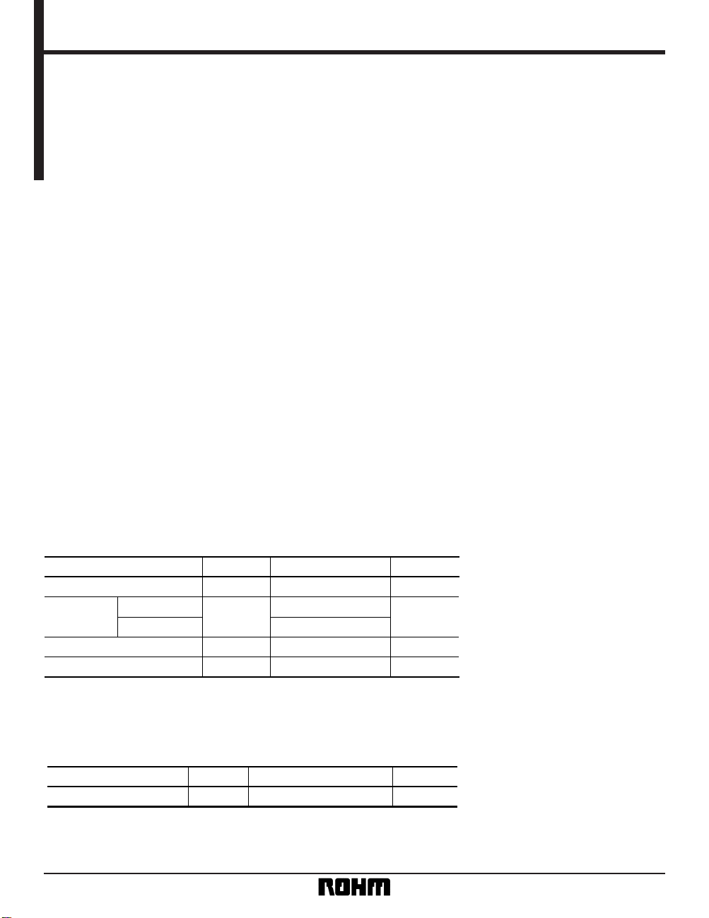
Absolute maximum ratings (Ta = 25°C)
Parameter Symbol Limits Unit
Power supply voltage V
CC 13 V
Power
dissipation
BA7725S 1000
∗
1
mW
600
∗
2
BA7725FS
Storage temperature °C
Operating temperature °C
– 55 ~ + 125
– 10 ~ + 70
Pd
Tstg
Topr
∗
1 Reduced by 10mW for each increase in Ta of 1°C over 25°C.
∗
2 Reduced by 6.0mW for each increase in Ta of 1°C over 25°C.
•
Recommended operating conditions
Parameter Symbol Limits Unit
Power supply voltage VV
CC 6.5 ∼ 12.0
Page 2
2
Multimedia ICs BA7725S / BA7725FS
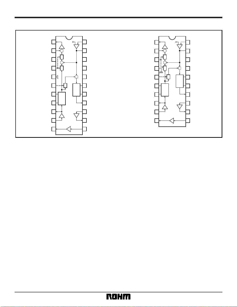
•
Block diagram
BA7725S BA7725FS
22
21
20
19
18
17
16
15
14
13
12
10
9
8
7
6
5
4
3
2
1
20
19
18
17
16
15
14
13
12
11
11
1
2
3
4
5
6
7
8
9
10
SW VR
VR
BF
EXPAND
BF
BF
BF
BF
EXPAND
VR
VRSW
MIC AMP IN
MIC AMP OUT
N.C.N.C.
GND
GND
DLY BF OUT
EXP BF IN
EXP BF OUT
EXP DET CT
EXP DET
LOOP GAIN CTRL
ECHO LEV CTRL
LINE IN
LINE OUT
COMPRESS
COMPRESS
RIPPLE FILTER
CMP DET
CMP DET CT
CMP OUT
CMP BF IN
CMP BF OUT
DLY BF IN
LINE OUT
LINE IN
ECHO LEV CTRL
LOOP GAIN CTRL
EXP DET
EXP DET CT
EXP BF OUT
EXP BF IN
DLY BF OUT
MIC AMP IN
MIC AMP OUT
RIPPLE FILTER
CMP DET
CMP DET CT
CMP OUT
CMP BF IN
CMP BF OUT
DLY BF IN
VCC
+
+
+
+
+
+
VCC
BF
Page 3
3
Multimedia ICs BA7725S / BA7725FS
•
Pin descriptions
Pin name Function
BA7725S BA7725FS
1 1 LINE OUT Line output
2 2 LINE IN Line input
3— —
—
N.C.
4 3 ECHO LEV CTRL
Microphone turns off when voltage drops below 1V.
Set echo signal damping ratio between 2-9V (Vcc = 9.0V).
5 4 GND Ground
6 5 LOOP GAIN CTRL
Setting the loop damping ratio. Set between
2-9V (Vcc = 9.0V).
7 6 EXP DET Expand detection
8 7 EXP DET CT
9 8 EXP BF OUT LPF BF output (expansion)
10 9 EXP BF IN LPF BF input (expansion)
11 10 DLY BF OUT Echo signal input BF output
12 11 DLY BF IN Echo signal input BF input
13 12 CMP BF OUT LPF BF output (compression)
14 13 CMP BF IN LPF BF input (compression)
15 14 CMP OUT Compression output
16 15 CMP DET CT
17 16 CMP DET Compression detection
18 17 RIPPLE FITER Attached ripple rejection capacitor
19 18
20 — N.C.
21 19 MIC AMP OUT Microphone amplifier output
22 20 MIC AMP IN Microphone amplifier input
Setting expand attack / recovery time
Attack (R) = 5.6kΩ, recovery (R) = 85.6kΩ
Setting the compression attack / recovery time
Attack (R) = 5.6kΩ, recovery (R) = 85.6kΩ
V
CCVCC
Pin No.
Page 4

4
Multimedia ICs BA7725S / BA7725FS
•
Input / output circuits
Pin name Pin No. Equivalent circuit
ECHO LEVEL
CTRL
4
LOOP GAIN
CTRL
6
Note: The BA7725FS is mounted on a 20-pin SSOP-A package with a different pin number than the BA7725S.
On the BA7725FS, the ECHO LEVEL CTRL pin is pin 3, and the LOOP GAIN CTRL pin is pin 5.
4
6
Page 5

5
Multimedia ICs BA7725S / BA7725FS
•
Electrical characteristics (unless otherwise noted, Ta = 25°C, Vcc = 9V)
Parameter Symbol Min. Typ. Max. Unit Conditions
Supply current I
CC
4.3 5.7 7.6 mA No input
Line through output level V
OLL
– 9.0 – 8.0 – 7.0 dBV VIN = – 26.0dBV
Line through output distortion THD
LL
— 0.15 0.5 %
Line through maximum output level V
OML
+ 5.0 + 7.2 — dBV
Line through noise level V
ONL
— – 92 – 77 dBV
Microphone through output level V
OML
– 10.5 – 8.5 – 6.5 dBV VIN = – 52dBV
Microphone through output distortion THD
ML
— 0.2 0.5 %
Microphone through input conversion noise V
ONM
— – 114 – 104 dBV Input shorted
Microphone through crosstalk CT
ML
— – 91 – 75 dBV
Compress output level V
OMC
– 6.5 – 4.5 – 2.5 dBV VIN = – 52dBV
Compress output distortion THD
MC
— 0.5 2.0 %
Compress noise level V
ONC
— – 55 – 45 dBV
Compress characteristics CMP — – 11.0 — dB
V
ODL1
– 11.7 – 9.7 — dBV VIN = – 5.0dBV, V4 = 9.0V
Expand output distortion THD
DL
— 0.25 2.0 %
Expand characteristic EXP — – 19.5 — dB
V
ODL2
— – 54 – 44 dB
V
ODC1
– 7.5 – 5.5 — dBV VIN = – 5.0dBV, V6 = 9.0V
V
ODC2
— – 42 – 32 dBV
MIC OFF holding voltage V
4OFF
0.0 — —
—
1.0 V
MIC ON holding voltage V
4ON
2.0 — 9.0 V
V
IN
= – 42dBV → – 62dBV
Output level differential
Expand output level 1
Expand output level 2
V
IN
= 0dBV → – 10.0dBV
Output level differential
V
IN
= – 5.0dBV,
Output level differential relative to Vo
DL1
VIN = – 5.0dBV,
Output level differential relative to Vo
DC1
Loop output level 1
Loop output level 2
〈
LINE THROUGH〉 INPUT : LINE IN, OUTPUT : LINE OUT
〈
MIC THROUGH〉 INPUT : MIC AMP IN, OUTPUT : LINE OUT
〈
COMPRESS〉 INPUT : MIC AMP IN, OUTPUT : CMP BF OUT
〈
EXPAND〉 INPUT : DLY BF IN, OUTPUT : LINE OUT
〈
Loop〉 INPUT : DLY BF IN, OUTPUT : CMP BF OUT
〈
Mode holding voltage
〉
Unless otherwise noted, V4 = 9.0V (MIC ON), V6 = 9.0V (Max. LOOP GAIN)
∗
1 BW = 0.4-30kHz
∗
2 DIN AUDIO
V6 = 2.0V (VR = Min. time)
V
4
= 2.0V (VR = Min. time)
V
IN
= – 26.0dBV, MIC OFF,
∗
1
MIC OFF, Rg = 600Ω,
∗
2
VIN = – 52dBV,
∗
1
V
IN
= – 44dBV, MIC OFF,
∗
2
V
IN
= – 52dBV,
∗
1
Rg = 600Ω,
∗
2
V
IN
= – 5.0dBV, V
4
= 9.0V,
∗
1
THD = 1%,
∗
1
Page 6

6
Multimedia ICs BA7725S / BA7725FS
•
Measurement circuit
BF
BF
BF
VR
VRSW
EXPAND
12345 78910116
17 12131415161819202122
V4 V6
+
+
R17
C15
R13
C14
R16
C18
R34
1k
C33
R11
C10
R9
C12
R8
+++
COMPRESS
0.1µ
MIC AMP IN
R2
2.2kR382k
C1
1µ
C4
22µ
C5
0.1µC60.47µ
C32
0.1µ
R35
10k
DLY BF IN
CMP BF OUT
+
C30
2.2µ
C20
0.1µ
R31
10k
R33
1k
LINE
OUT
LINE
IN
C20
0.1µ
C19
0.47µ
++
VCC 9V
Fig.1
The above measurement circuit applies to a BA7725S mounted to a 22-pin SDIP package. A BA7725FS mounted to a 20pin SSOP-A package lacks N.C. pins 3 and 20; other than this
difference, the above circuit diagram applies.
•
Circuit operation
(1) MIC AMP IN / LINE OUT gain
Microphone amplifier gain (determined by R9 and R10) + line
amplifier gain (+12dB)
The audio signal is input via pin 22 (BA7725S) or pin 20
(BA7725FS) and amplified by the internal microphone amplifier, whose gain can be set with (attached) R9 and R10.
Note: Microphone amplifier gain must be set above +15dB.
Microphone amplifier frequency
characteristic measurement circuit
–
+
Fig.2
1.5k 12k
22 21
BA7725S
VoutVIN
60
50
40
30
20
10
0
– 10
–20
–30
– 40
1M
10M
24681 1864218642
Open loop gain
10k 100k
Frequency characteristic (Hz)
Voltage (dB)
Microphone amplifier frequency
characteristics
Fig.3
++
+
+ 18dB
+
Fig.4
21
2122
MIC AMP IN
R9 R10
SW
LINE OUT LINE IN
Page 7

7
Multimedia ICs BA7725S / BA7725FS
105
– 100
–50
0
Secondary echo
Sound source
Primary echo
0
ATT (dB)
V
4 = 9.0V
LOOP GAIN CTRL pin voltage : (V)
Line output attenuation vs.
loop gain control pin voltage
Line output attenuation : A
TT
(dB)
Fig.7
0
– 50
– 100
0510
Primary echo
Sound source
ATT (dB)
ECHO LEVEL CTRL pin voltage : (V)
Line output attenuation vs.
echo level control pin voltage
Line output attenuation : A
TT
(dB)
Fig.6
(2) LINE IN / LINE OUT gain
Line amplifier gain is fixed at +18dB.
+
+
+
+
+12dB
Fig.5
21
2122
MIC AMP IN
R9 R10
SW
LINE OUT LINE IN
After being amplified by the internal microphone amplifier, the audio signal is logarithmically compressed by 1 / 2 then input to the tertiary low pass filter, which
comprises an internal BF and attached capacitor and resistor.
(3) Echo level control
The DC voltage supplied to pin 4 (BA7725S) or pin 3 (BA7725FS) determines
when the microphone switch is turned on and off and controls the echo level.
Line input and level-controlled microphone input are mixed and output.
Mode Threshold voltage Operation
L (1.0V Max.) Only line audio is output.MIC OFF
H (2.0V Min.)MIC ON
Microphone switch control
Echo level control
Attenuation of the primary echo signals from sound
source can be controlled by changing the DC voltage
impressed on pin 4 (BA7725S) or pin 3 (BA7725FS)
between 2V and 9V.
Attenuation of primary echo signals can be controlled
by changing the DC voltage impressed on pin 6
(BA7725S) or pin 5 (BA7725FS) .
Page 8

8
Multimedia ICs BA7725S / BA7725FS
A : Echo signal attenuation
B : Loop signal attenuation
C : Delay time
CCC
B
B
A
(dB)
(t)
Fig.8
Relationship between echo gain and loop gain
(4) Echo signal frequency characteristicis
The figure below shows the attenuation of signals output from pin 1 when the audio signal is input to pin 22
(BA7725S) or pin 20 (BA7725FS). (This is the attenuation when the input signal is output without being
passed through the BU9252S / F, and when the primary and secondary echo signals are passed through an
attached low pass filter with the same constant shown
in "Application example," and then processed by the
BU9252S / F delay circuit.)
Note: These are the values when using the constant shown in "Application
example."
0
–10
–20
–30
– 40
– 50
100 1k 10k 100k
Sound source
Secondary echo signal
SIGNAL FREQUENCY : f (Hz)
—
3pin, 5pin = VCC (VR : Max.)
Echo signal frequency
characteristics
LINE OUTPUT ATTENUATION : A
TT
(dB)
Fig.9
Primary echo signal
•
External dimensions (Units: mm)
SDIP22 SSOP-A20
3.95 ± 0.3
0.51Min.
19.4 ± 0.3
3.4 ± 0.2
0.5 ± 0.1
6.5 ± 0.3
1
11
1222
0.3
± 0.1
0° ~ 15°
1.778
7.62
BA7725S BA7725FS
11
10
20
1
0.11
7.8 ± 0.3
5.4 ± 0.2
8.7 ± 0.2
0.15 ± 0.1
0.36 ± 0.10.8
1.8 ± 0.1
0.3Min.
0.15
 Loading...