

Page 1
1
Multimedia ICs
3-channel 75Ω driver with Y / C MIX
BA7665FS
The BA7665FS has three 75Ω driver circuits with 6dB amplifiers, and includes a Y / C MIX circuit. The IC can provide a 75Ω drive with a composite Y signal, C signal, or a Y / C MIX signal. Dual-circuit drive capacity for each load
is provided, and a sag compensation function is provided to allow use of smaller coupling capacitors.
The composite Y signal input is a sync-tip clamp input, and the chroma input is a biased input.
The three channels can be simultaneously muted, or the chroma signal only (in the case of C / Y output, only Y is
output), and output short circuit protection and power save circuits are also provided.
•
Applications
Digital AV equipment, DVD and DVC players
•
Features
1) Y / C MIX circuit.
2) Low power consumption (typ. 130mW).
3) Output mute circuit.
4) Power save circuit.
5) Output protection circuit.
6) Sag compensation circuit allows small output coupling capacitors.
7) Two-circuit drive possible for loads.
8) Compact SSOP-A 16-pin package.
•
Absolute maximum ratings (Ta = 25°C)
Parameter Symbol Limits Unit
Power supply voltage
Power dissipation
Operating temperature
Storage temperature
V
CC
Pd
Topr
Tstg
8
650
∗
– 25 ~ + 75
– 55 ~ + 125
V
mW
°C
°C
∗
Reduced by 6.5mW for each increase in Ta of 1°C over 25°C.
•
Recommended operating conditions (Ta = 25°C)
Parameter Symbol UnitMax.Typ.Min.
Power supply voltage
V
CC 4.5 5.55.0 V
䊊 Not designed for radiation resistance.
Page 2
2
Multimedia ICs BA7665FS
•
Electrical characteristics (unless otherwise noted, Ta = 25°C, VCC = 5V)
Parameter
Symbol Min. Typ. Max. Unit Conditions
Circuit current
Maximum output level
Frequency characteristics
Inter channel crosstalk
Mute attenuation
Mute switch high level
Mute switch low level
Input impedance
I
CC
Vom
Gf
CT
MT
VTHH
VTHL
ZIN
13.0
2.6
– 1.0
—
—
2.5
0
16
26.0
3.0
0.0
– 60
– 60
—
—
20
39.0
—
1.0
—
—
V
CC
1.0
24
mA
V
P-P
dB
dB
dB
V
V
kΩ
No signal
f = 1kHz, THD = 1 %
f = 7MHz / 1MHz, 1V
P-P
f = 4.43MHz, 1VP-P
f = 4.43MHz, 1VP-P
Chroma input pin (pin 7)
•
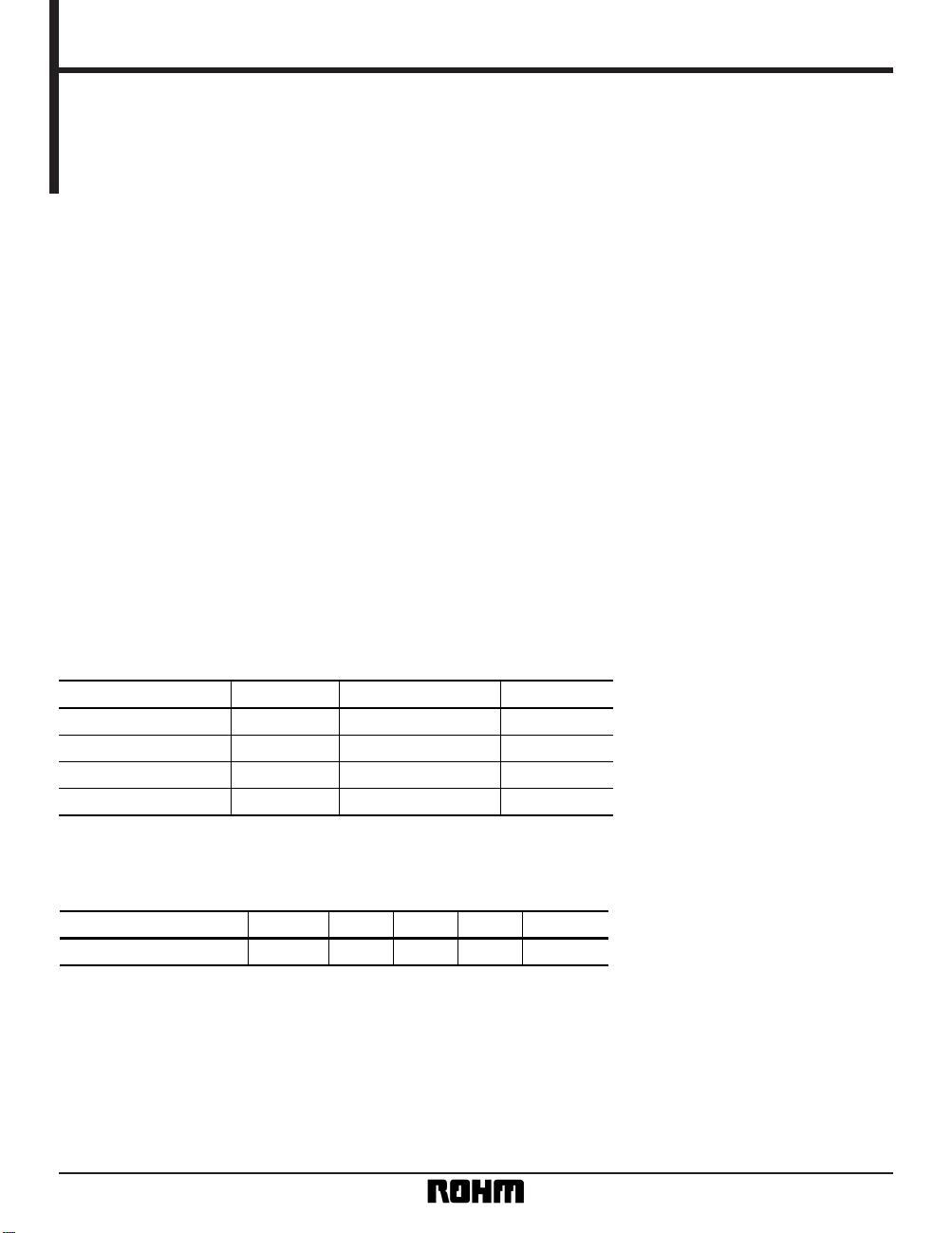
Block diagram
+
6dB
Mute
75Ω
6dB 75Ω
6dB 75Ω
20k
1
2
3
4
5
6
7
8
MUTEA
INA
GND
GND
GND
N.C.
INB
MUTEB
16
15
14
13
12
11
10
9
V
CC1
OUTA1
OUTA2
V
CC2
MIXOUT1
MIXOUT2
N.C.
OUTB
Chroma Mute
Page 3
3
Multimedia ICs BA7665FS
•
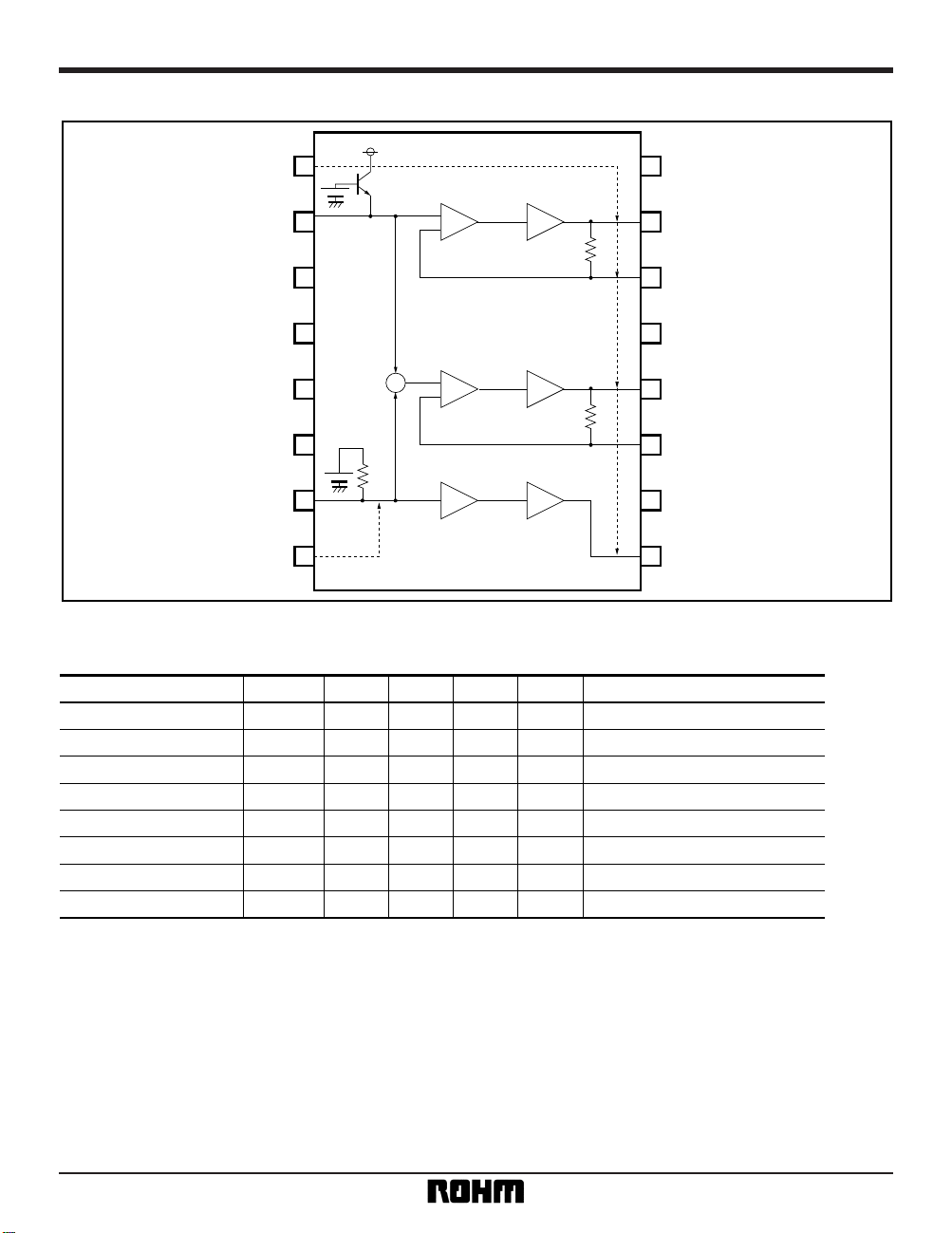
Measurement circuit
+
6dB
Mute
75Ω
6dB 75Ω
6dB 75Ω
N.C.
N.C.
20k
+
++
100µF
22µF
0.1µF47µF
1
3.3V
1.2V
2
3
4
5
6
7
8
16
15
14
13
12
11
10
9
Chroma Mute
A
V
++
100µF
22µF
V
0.1µF
V
SW16
1
2
75Ω
75Ω
75Ω
1
1
2
2
3
SW1
SW2
+
1µF
+
1µF
1
2
3
1
2
3
0.1µF
0.1µF
3.3V
1.2V
SW7
SW8
V
Fig.1
Page 4

4
Multimedia ICs BA7665FS
•
Measurement conditions
Parameter
Symbol
Measurement
method
Switch conditions
Circuit current
Maximum
output level
Frequency
characteristics
Crosstalk
Mute attenuation
Chroma mute attenuation
Input impedance
Voltage gain
Inter-channel
voltage gain differential
ICC
VOM1
VOM2
VOM3
GF1
GF2
GF3
GT1
GT2
MT1
MT2
MT3
MTC1
MTC2
ZIN
GV1
GV2
GV3
∆GVC
OUTA
MIXOUT
OUTB
OUTA
MIXOUT
OUTB
OUTB→OUTA
OUTA→OUTB
OUTA
MIXOUT
OUTB
MIXOUT
OUTB
OUTA
MIXOUT
OUTB
Note 1
Note 2
Note 3
Note 4
Note 5
Note 5
Note 6
Note 7
Note 8
SW
1
2
3
3
3
3
3
3
3
3
1
1
1
3
3
3
3
3
3
—
SW
2
1
2
2
1
2
2
1
1
2
2
2
1
1
1
1
2
2
1
—
SW
7
1
1
1
2
1
1
2
2
1
1
1
2
2
2
3
1
1
2
—
SW
8
2
3
3
3
3
3
3
3
3
3
3
3
1
1
3
3
3
3
—
SW
16
1
2
2
2
2
2
2
2
2
2
2
2
2
2
2
2
2
2
—
∗
The mute switch level was substituted by using H = 2.4V and L = 1.1V for the above measurements.
—
—
Measurement method
Note 1: Measure the quiescent current.
Note 2: Connect a distortion meter to the output, and input a f = 1kHz sine wave.
Adjust the output level until the output distortion is 1%. The output voltage at this time is the maximum output level V
OM [VP-P].
Note 3: Input 1V
P-P, 7MHz and 1MHz sine waves, and measure the corresponding outputs VO7 and VO1. The frequency characteristic is given by
G
F = 20
∗
Log (VO7 / VO1) [dB].
Note 4: Input a 1V
P-P, 4.43MHz sine wave, and measure the output Vo [VP-P] The interchannel crosstalk is given by CT = 20
∗
Log (VO / VIN) [dB].
Note 5: Input a 1V
P-P, 4.43MHz sine wave, and measure the output Vo [VP-P] The mute attenuation is given by
M
T = 20
∗
Log (VO / VIN) [dB].
Note 6: Measure the input pin voltage V
IN50 when a current of DC50µA is flowing into the input pin. Measure the input pin open-circuit voltage.
The input impedance is given by
Z
IN = | VIN50 – VIN0 | / 50
∗
103[kΩ].
Note 7: Input a 1V
P-P, 4.43MHz sine wave, and measure the output VO [VP-P] The voltage gain is given by
Gv = 20 ∗log (V
O / VIN) [dB].
Note 8: ∆G
VC = | GV1 – GV2 | [dB]
Page 5

5
Multimedia ICs BA7665FS
Parameter
Symbol Min. Typ. Max. Unit Conditions
Voltage gain
Interchannel voltage gainGv∆Gv
5.5
– 0.5
6.0
0.0
6.5
0.5
dBdBf = 4.43MHz, 1VP-P
f = 100kHz, 1VP-P
•
Guaranteed design values (unless otherwise noted, Ta = 25°C, VCC = 5V)
•
Mute SW mode settings
3ch MUTE
• MUTEA (1pin)
H
NORMALL
CHROMA MUTE
• MUTEB (8pin)
H
NORMALL
•
Pin descriptions and equivalent I / O circuits
Pin. No Pin name IN OUT
Standard potential
Equivalent I / O circuit Pin description
1 MUTEA
MUTEB
K ——
K — 2.0V
K — 2.0V
—— 0V
1
8
2
7
3
4
5
INA
INB
GND
Mute control pin
When MUTE A (pin 1) goes high, all
three channels are muted at the same
time. When MUTE B (pin 8) goes
high, OUTB and the MIXOUT chroma
signals are muted.
Signal input pin
This is the input pin for the composite
Y signal (sync-tip clamp input).
Ground pin
Signal input pin
Bias-type input pin for the chroma
signal. The input impedance is 20kΩ.
15k
8k
20k
↓
↓
GND
Page 6

6
Multimedia ICs BA7665FS
Pin. No Pin name IN OUT
Standard voltage
Equivalent I / O circuit Pin description
9 OUTB — K 2.4V
— K
0.9V
0.95V
1112MIXOUT2
MIXOUT1
— K
0.9V
0.95V
14
15
OUTA2
OUTA1
——
5.0V
5.0V
13
16
V
CC2
V
CC1
Signal output pin
Chroma signal output pin. When this
drops below 0.2V, the protection
circuit operates and the IC enters
power save mode.
Signal output pin
Y / C signal output pin. Pin 11 is the
sag compensation pin. When pin 12 is
taken below 0.2V, the protection circuit operates and the IC enters power
save mode.
Signal output pin
Composite Y signal output pin. Pin 14
is the sag compensation pin. When
pin 15 is taken below 0.2V, the
protection circuit operates and the IC
enters power save mode.
Power supply pin
V
CC1 and VCC2 are not connected
internally. Use with them connected
externally.
11pin
12pin
14pin
15pin
VCC
Page 7

7
Multimedia ICs BA7665FS
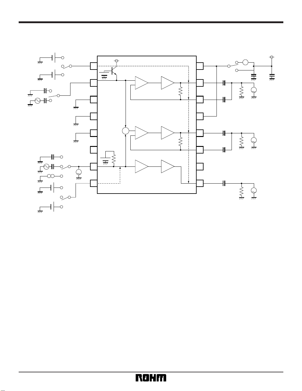
+
6dB
Mute
75Ω
6dB 75Ω
6dB 75Ω
6dB 75Ω
N.C.
20k
N.C.
+
+
++
75Ω
75Ω
75Ω
75Ω
100µF
22µF
++
75Ω
+
75Ω
100µF
75Ω
75Ω
0.1µF
1000µF
22µF
47µF
1µF
0.1µF
0.1µF
1
2
3
4
5
6
7
8
16
15
14
13
12
11
10
9
Composite Y
Chroma
Chroma Mute
When you will not use the sag compensation function
Fig.2
•
Application example
Page 8

8
Multimedia ICs BA7665FS
SSOP-A16
0.36 ± 0.10.8
0.11
6.6 ± 0.2
4.4 ± 0.2
6.2 ± 0.31.5 ± 0.1
1
16
8
9
0.15
0.3Min.
0.15 ± 0.1
•
External dimensions (Units: mm)
 Loading...