

Page 1
1
Multimedia ICs
2-input, 1-output video signal
switcher
BA7654F
The BA7654F is video signal switch consisting of two input pins (IN1 and IN2), one CTL pin (CTL), and one output
pin (OUT). The inputs are sync-tip clamped (synchronous edge of the video input signals are aligned to the same
voltage), and as the input impedance is extremely large, it is possible to use a small value for the clamp capacitor
(the recommended capacitor is 0.01µF (FZ) ceramic).
•
Applications
VCRs, TVs, and other equipment using video signals
•
Features
1) Small clamp capacitors can be used (ceramic,
3000pF (Min.), 0.01µF (FZ) (recommended)).
2) Low supply voltage operation possible supply voltage range is 3.7V to 7.7V.
3) Superimposition used for fast switching speed with
low switching noise (70ns Typ.).
4) Low power consumption
(when V
CC = 5V, 25mW Typ.).
5) Wide dynamic range (when V
CC = 5V, 3.1VP-P Typ.).
6) Excellent frequency characteristics (10MHz, 0dB
Typ.).
7) Low interchannel crosstalk (– 70dB Typ.).
8) Voltage can be applied to the control pins even
when V
CC is not applied.
•
Selected output mode setting table
CTL OUT
L IN1
H IN2
•
Absolute maximum ratings (Ta = 25°C)
Parameter Symbol Limits
9
500
∗
– 25 ~ + 75
– 55 ~ + 125
Unit
V
mW
°C
°C
V
CC
Pd
Topr
Tstg
Applied voltage
Power dissipation
Operating temperature
Storage temperature
∗
Reduced by 50mW for each increase in Ta of 1°C over 25 °C.
•
Recommended operating conditions (Ta = 25°C)
Parameter Symbol Limits
4.0
~ 7.0
Unit
VV
CCOperating power supply voltage
䊊Not designed for radiation resistance.
Page 2
2
Multimedia ICs BA7654F
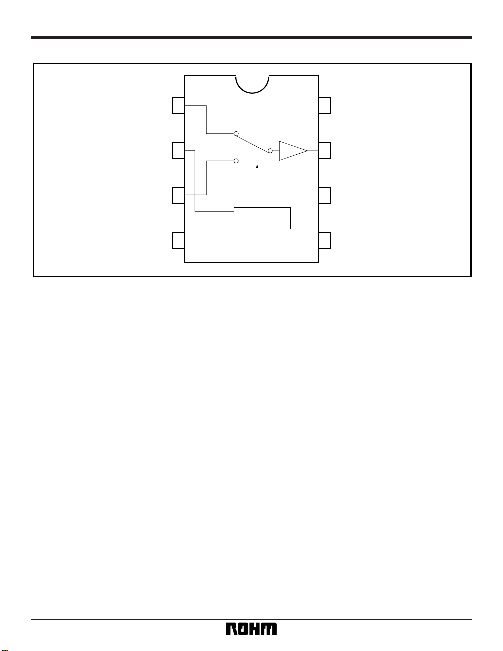
•
Block diagram
1IN1 GND8
2CTL OUT7
3IN2 VCC6
4GND Open.5
Logic
Page 3
3
Multimedia ICs BA7654F
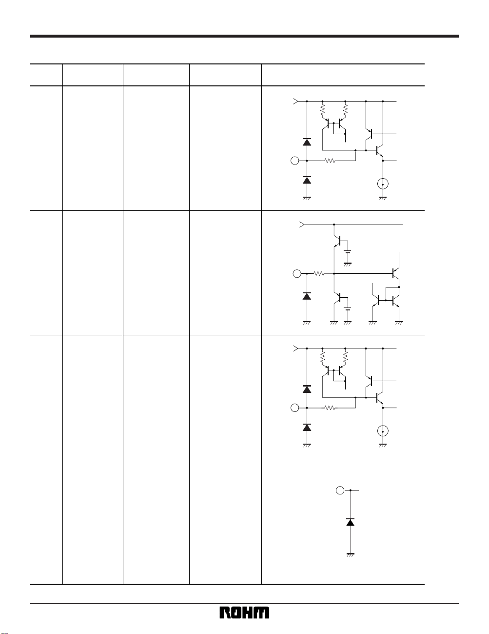
•
Input / output circuits (1 / 2)
Vcc
IN1
100
50µA
Pin
No.
Pin name
Reference voltage
(V
CC = 5V)
Input/output
impedance
1 1.65VIN 1 10MΩ or more
2—CTL —
3 1.65VIN 2 10MΩ or more
4—GND —
Equivalent circuit
Vcc
CTLa
1.9V
50k
2.3V
Vcc
IN1
100
50µA
GND
Page 4

4
Multimedia ICs BA7654F
•
Input / output circuits (2 / 2)
Pin
No.
Pin name
Reference voltage
(V
CC = 5V)
Input/output
impedance
6 0.5VV
CC —
7 0.95VOUT 26Ω
80VGND —
Equivalent circuit
Vcc
OUT
ImA
Vcc
Vcc
GND
Page 5

5
Multimedia ICs BA7654F
•
Electrical characteristics (unless otherwise noted, Ta = 25°C, VCC = 5V)
Parameter Symbol Min.
3.7
2.7
2.6
– 0.5
Typ.
—
5.0
3.1
0
Max.
7.7
8.2
—
+ 0.5
V
CC
ICC
Vom
G
V
Power supply voltage
Circuit current
Maximum output level
Voltage gain
Interchannel crosstalk
Frequency characteristics
CTL switching voltage
Unit
V
mA
V
P-P
dB
Conditions
f = 1kHz, THD = 1.0%
f = 1MHz, VIN = 1.0VP-P
– 3.0 0 + 1.0 Gf dB
V
∗
f = 10MHz/1MHz, VIN = 1.0VP-P
— — 1.0VthL
2.5 — —VthH
— – 70 —Cta dB f = 4.43MHz, V
IN = 1.0VP-P
∗
Vcc-CTL Threshold Level
Vth = ×
20 (V)
Vcc-VF
45
—
—
•
Guaranteed design parameters (unless otherwise noted, Ta = 25°C, VCC = 5V)
Parameter Symbol Min.
—
Typ.0Max.
0.5DG
Differential gain
Differential phase
Unit
%
— 0.5 1.0DP deg
Conditions
V
IN = 1.0VP-P
standard staircase signal
V
IN = 1.0VP-P
standard staircase signal
•
Measurement circuit
1
8
2
7
3
6
4
5
Logic
Clump
Clump
SW7
12
Vector
Scorp
Vcc
SW2
12
47µ0.1µ
C11C10
Open
2.5V1.0V
SW1
12
OSC
C1 C23C3
3300p 3300p 3300p
1.0V
V
A
SG
SW3
12
OSC
C4 C53C6
3300p 3300p 3300p
SG
Fig. 1
Page 6

6
Multimedia ICs BA7654F
Parameter
Circuit current
Voltage gain
Frequency
characteristics
Interchannel
crosstalk
Differential gain
Differential phase
Maximum
output level
IN 1
IN 2
IN 1
IN 2
IN 1
IN 2
IN 1→IN 2
IN 2←IN 1
IN 1
IN 2
IN 1
IN 2
Symbol SW1 SW3 SW2
SW7 Conditions
Icc 3 3 2 — —
f = 1kHZ THD = 1.0%
∗
1
VIN = 1.0VP-P f = 1MHz
∗
2
VIN = 1.0VP-P f = 1MHz and 10MHz
∗
3
VIN = 1.0VP-P f = 4.43MHz
∗4
VIN = 1.0VP-P standard staircase signal
V
IN = 1.0VP-P standard staircase signal
Vom 1
Vom 2
Gv 1
Gv 2
Gf 1
Gf 2
Cta1 – 2
Cta2 – 1
D
G 1
D
G 2
DP 1
D
P 2
1
3
1
3
1
3
1
3
2
3
2
3
3
1
3
1
3
1
3
1
3
2
3
2
1
2
1
2
1
2
2
1
1
2
1
2
1
1
1
1
1
1
1
1
2
2
2
2
∗
CTL switching level is substituted by performing the above measurements.
∗
1 Connect a distortion meter to the output. After adding a f = 1kHz sine wave input from the OSC, adjust the input level so that the output
distortion is 1.0%. The output voltage at that time is the maximum output level Vom [VP-P].
∗
2 Apply to the input pin a VIN = 1.0VP-P, f = 1MHz sine wave input.
Voltage gain GV = 20-log (VOUT / VIN)
∗
3 Apply to the input pin VIN = 1.0VP-P, f = 1MHz and 10MHz sine wave inputs.
Frequency characteristics Gf = GV (f = 1MHz) – GV (f = 10MHz)
∗
4 Apply to the input pin a VIN = 1.0VP-P, f = 4.43MHz sine wave input.
Interchannel crosstalk Cta = 20log (VOUT / VIN)
•
Measurement conditions
Page 7

7
Multimedia ICs BA7654F
1
C.Video IN
6
3
5 7
2
4
IN 1
BA7654F
C.Video OUT
IN 2
Open
CTL
GND
Vcc
OUT
GND
8
0.01µ
C.Video IN
0.01µ
Logic
0.1µ47µ
Vcc
Fig. 2
•
Application examples
1
6
3
5
7
2
4
IN 1
BA7654F
C.Video OUT/DC OUT
IN 2
Open
CTL
GND
Vcc
OUT
GND
Fig. 3
8
DC 1.7V(min)
Logic
C.Video IN
0.01µ
0.1µ47µ
Vcc
Page 8

8
Multimedia ICs BA7654F
•
Operation notes
(1) To ensure stable clamp operation, the output
impedance of the previous stage connected to the
inputs should be 1kΩ or lower.
(2) If large input clamp capacitors are used, the time
constant of the circuit will mean that some time will be
required until stable operation after power is applied.
The value for the input clamp capacitors is 0.1µF max.
(0.01µF (FZ) ceramic capacitor recommended).
(3) If CTL pins are unstable when open. Set them to
either H or L.
(4) When using superimposition, the DC voltage directly applied to the inputs should be at least 1.7V.
QFP44
33 23
22
12
1
34
44
10.0 ± 0.2
14.0 ± 0.3
0.35 ± 0.1
10.0 ± 0.2
14.0 ± 0.3
1.2
0.05
2.15 ± 0.1
0.15 ± 0.1
0.8
11
0.15
•
External dimensions (Units: mm)
 Loading...