

Page 1
1
Multimedia ICs
Video switch for CANAL-Plus decoder
BA7631 / BA7631F
The BA7631 and BA7631F are audio-switching ICs for decoders for scrambled pay channels used in France and
other countries. The ICs include a five-input multiplexer, a four-input multiplexer and a two-input multiplexer, and
allow decoder audio switching to be done with a single IC. When used in combination with the BA7630S common
logic control can be used for audio and video switching.
•
Applications
Video cassette recorders
•
Features
1) All the audio-switching functions required for SECAM
CANAL -plus decoder integrated onto one chip.
2) Inputs terminated with 65kΩ resistors.
3) Built-in output buffer.
4) Wide supply voltage range (4.5V to 13.0V).
5) Low total harmonic distortion (0.005% Typ.).
6) Wide dynamic range (3.6Vrms, V
CC = 12V).
7) Same control logic as for the BA7630S can be used.
•
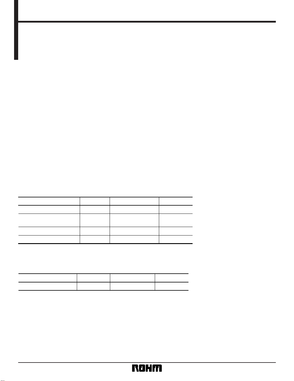
Absolute maximum ratings
Parameter
Symbol
Limits Unit
V
CC
13.5 V
mV
°C
°C
1100
∗
(DIP)
500
∗
(SOP)
– 55 ~ + 125
– 25 ~ + 70
Pd
Topr
Tstg
∗
Reduced by 11mW (DIP) or 5mW (SOP) for each increase in Ta of 1°C over 25°C.
Applied voltage
Power dissipation
Operating temperature
Storage temperature
•
Recommended operating conditions (Ta = 25°C)
Parameter Symbol Limits Unit
V
CC
4.5 ~ 13.0 VPower supply voltage
Page 2
2
Multimedia ICs BA7631 / BA7631F
•
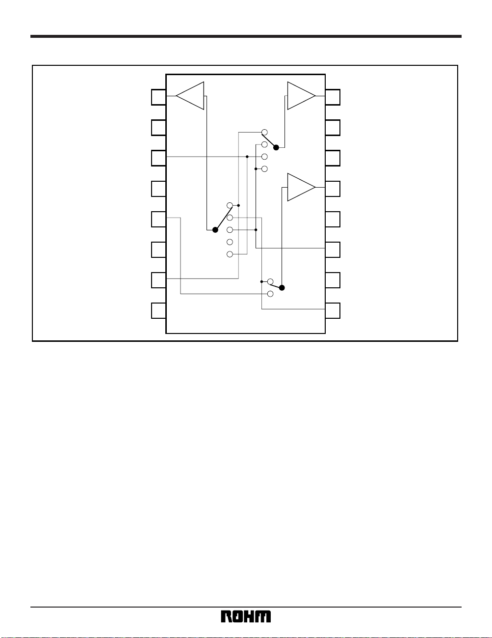
Block diagram
1
2
3
4
5
6
7
89
10
11
12
13
14
15
16
BF
BF
BF
1
2
3
4
SW2
1
2
3
4
5
SW1
1
2
SW3
BA7631
OUT1
CTL4
IN5
V
CC
IN4
GND2
IN1
CTL1
OUT2
CTL5
CTL3
OUT3
CTL2
IN3
GND1
IN2
Page 3
3
Multimedia ICs BA7631 / BA7631F
•
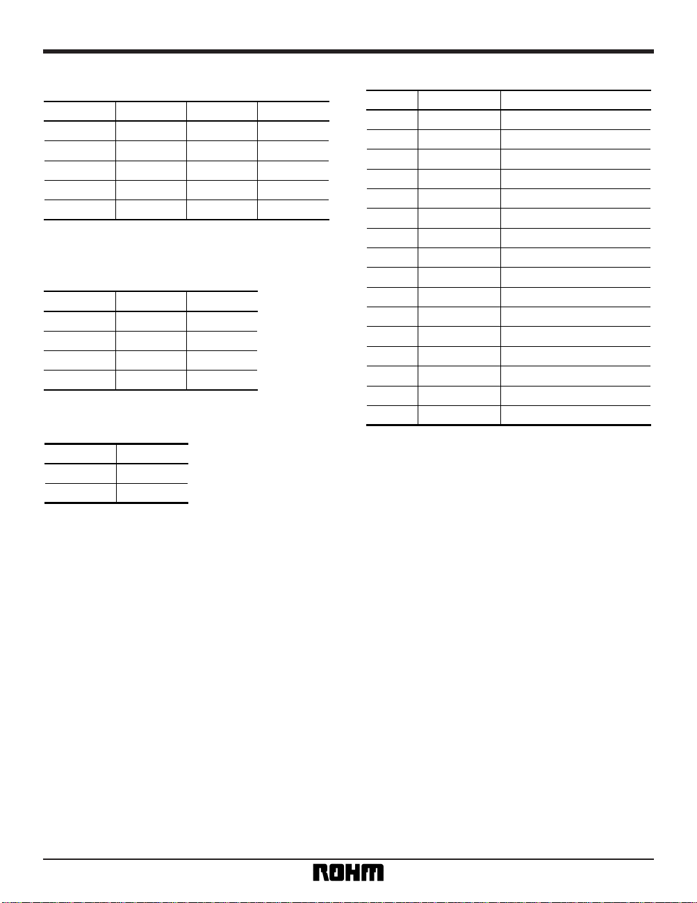
Truth table
•
Pin descriptions
CTL1 CTL2 CTL5 SELECT
LLLIN1
L H L IN2
H L L IN3
H H L MUTE
∗∗H IN5
OUT1 SW1 block
∗
Don't care
CTL3 CTL5 SELECT
LL
HL
LH
HH
IN1
IN3
IN5
IN3
OUT2 SW2 block
CTL4 SELECT
L
H
IN2
IN4
OUT3 SW3 block
1
2
3
4
5
6
7
8
9
10
11
12
13
14
15
16 OUT2
CTL5
CTL3
OUT3
CTL2
IN3
GND1
IN2
CTL1
IN1
GND2
IN4
V
CC
IN5
CTL4
OUT1
Pin No.
FunctionPin name
Output 1
Control 4
Input 5
Power supply
Input 4
GND (GND1 common)
Input 1
Control 1
Input 2
GND (GND2 common)
Input 3
Control 2
Output 3
Control 3
Control 5
Output 2
Page 4

4
Multimedia ICs BA7631 / BA7631F
•
Input / output circuits
N
50
1.8mA
1
VCC
Q1
8
12
14
15
10k
30k
36k
14k
VCC
2
1.8mA
25
13
16
VCC
6.0V
125µA
100
30µA
VCC
3, 5, 7, 9, 11
65k
Page 5

5
Multimedia ICs BA7631 / BA7631F
•
Electrical characteristics (unless otherwise noted, Ta = 25°C and VCC = 12V)
Parameter
Symbol Min. Typ. Max. Unit
V
CC 4.5 12.0 13.0 V —
I
CC ——14.9 24.0 mA
V
om 3.1 3.6 — Vrms
GV – 0.5 0 0.5 dB
THD — 0.005 0.1 %
C
TM —– 75 – 60 dB
V
Min. — 20.0 40.0
µV
rms
VTH 1.0 2.0 3.0 V —
Z
IN 48.5 65 80.5
Conditions
kΩ —
f = 1MHz, THD = 0.5%
f = 1kHz, V
IN = 3.0dBm
f = 1kHz, V
IN = 3.0dBm
f = 10kHz, V
IN = 3.0dBm
30kHz LPF, R
g = 2.2kΩ
䊊Not designed for radiation resistance.
Recommended operating voltage
Circuit current
Maximum output level
Voltage gain
Total harmonic distortion
Interchannel crosstalk
Input conversion noise voltage
CTL switch level
Input impedance
•
Circuit operation
The BA7631 and BA7631F make it easy to construct a decoder for the scrambled pay channels. They have been
designed specifically for audio signal decoding. As shown in the application examples in Figs. 1 and 2, there are
inputs for TV, VCR, decoder, and AUX, to cover a wide range of applications. When the AUX input is not used, by
setting CTL5 to “L”, the system construction becomes the same as that of the BA7630S, and the BA7630S switching
logic can be used as is.
•
Application example
1
2
3
4
5
6
7
8
16
15
14
13
12
11
10
9
BF
BF
BF
1
2
3
4
SW2
SW1
1
2
3
4
5
1
2
SW3
22µF
22µF
22µF
22µF
22µF
22µF
47µ
22µF
from
V
CC
To VTR IN
CTL4 for SW3
from EXT OUT
from VTR OUT
from VTR
TUNER OUT
CTL1 for SW1
To DECODER IN
CTL5 for SW2
CTL3 for SW2
To TV IN
CTL2 for SW1
from TV OUT
DECODER OUT
Fig.1
++
+
+
+
+
+
+
Page 6

6
Multimedia ICs BA7631 / BA7631F
TUNER
IN
OUT
VTR
DECODER
IN
OUT
7
9
11
3
5
2
13
14
16
15
12
8
1
OUT
IN
TV
EXT
OUT
22µF
22µF
22µF
CTL1
CTL2
CTL3
CTL5
CTL4
SW1
BF
SW2
1
2
3
4
1
2
SW3
BF
BF
1
2
3
4
5
22µF
22µF
22µF
22µF
22µF
(AUX)
Fig.2
+
++
+
+
+
+
+
Page 7

7
Multimedia ICs BA7631 / BA7631F
•
Electrical characteristic curves
1.0 2.0 3.0 4.00
0.010
0.100
0.001
TOTAL HARMONIC DISTORTION (%)
VCC = 12.0 (V)
f = 1 (kHz)
INPUT VOLTAGE: (Vrms)
Fig. 3 Distortion characteristics
510150
1.0
2.0
3.0
4.0
5.0
Max. OUTPUT LEVEL (Vrms)
VCC = 12.0 (V)
f = 1 (kHz)
THD = 0.5 (%)
POWER SUPPLY VOLTAGE: (V)
Fig. 4 Power supply voltage vs. dynamic
range characteristics
•
External dimensions (Units: mm)
SOP16
0.51Min.
0.3
± 0.1
916
81
6.5 ± 0.3
3.2 ± 0.2
4.25 ± 0.3
0.5 ± 0.1
19.4 ± 0.3
2.54
0
° ~ 15°
7.62
DIP16
BA7631 BA7631F
0.4 ± 0.11.27
0.15
0.15 ± 0.1
0.3Min.
4.4 ± 0.2
6.2 ± 0.3
0.11
1.5 ± 0.1
1
16
10.0 ± 0.2
8
9
 Loading...