

Page 1
1
Multimedia ICs
Video switch for CANAL-Plus decoder
BA7630S / BA7630F
The BA7630S and BA7630F are decoder switching ICs for the scrambled broadcasts in France. The ICs include a 3input multiplexer, 2-input multiplexers with 6dB amplifiers, and a 9-bit serial-to-parallel converter.
These ICs greatly simplify decoder switching, and can be connected to a control microprocessor using just two lines.
•
Applications
Video cassette recorders
•
Features
1) All the switching functions required for SECAM
CANAL plus decoder integrated onto one chip.
2) Built-in 9-bit serial-to-parallel converter for decoder
and TV control reduces number of microprocessor
wiring connections required.
3) Inputs have a sync-tip clamp.
4) The switch section can be used independently.
5) Low power consumption off a 5V supply.
•
Absolute maximum ratings (Ta = 25°C)
Parameter Symbol Limits Unit
V
CC
9
∗
1
V
BA7630S 500
∗
2
mW
BA7630F 600
∗
3
Topr – 25 ~ + 70 °C
Tstg – 55 ~ + 125 °C
Pd
Power supply voltage
Power dissipation
Operating temperature
Storage temperature
∗
1 13V for switches 1 to 9.
∗
2 Reduced by 5.0mW for each increase in Ta of 1°C over 25°C.
∗
3 Reduced by 6.0mW for each increase in Ta of 1°C over 25°C.
•
Recommended operating conditions (Ta = 25°C)
Parameter Symbol Min. Typ. Max. Unit
V
CC 4.5 5.0 5.5 VPower supply voltage
Page 2
2
Multimedia ICs BA7630S / BA7630F
•
Pin descriptions
Pin No. Pin No.
1 IN 4 OUT 2
2 GND
3 IN 1
4 (5) RESET IN SW 5 OUT
5 (6) IN 2 SW 6 OUT
GND SW 7 OUT
IN 3 SW 8 OUT
SW 1 IN / OUT CLOCK IN
SW 2 IN / OUT DATA IN
SW 3 IN / OUT SW 9 OUT
OUT 3 OUT 1
6 (7)
7 (8)
8 (9)
9 (10)
10 (13)
11 (14)
V
CC
SW 4 IN / OUT
12 (15)
13 (16)
14 (17)
15 (20)
16 (21)
17 (22)
18 (23)
19 (24)
20 (26)
21 (27)
22 (28)
Pin name Pin name
Pin numbers in parentheses are for the BA7630F.
•
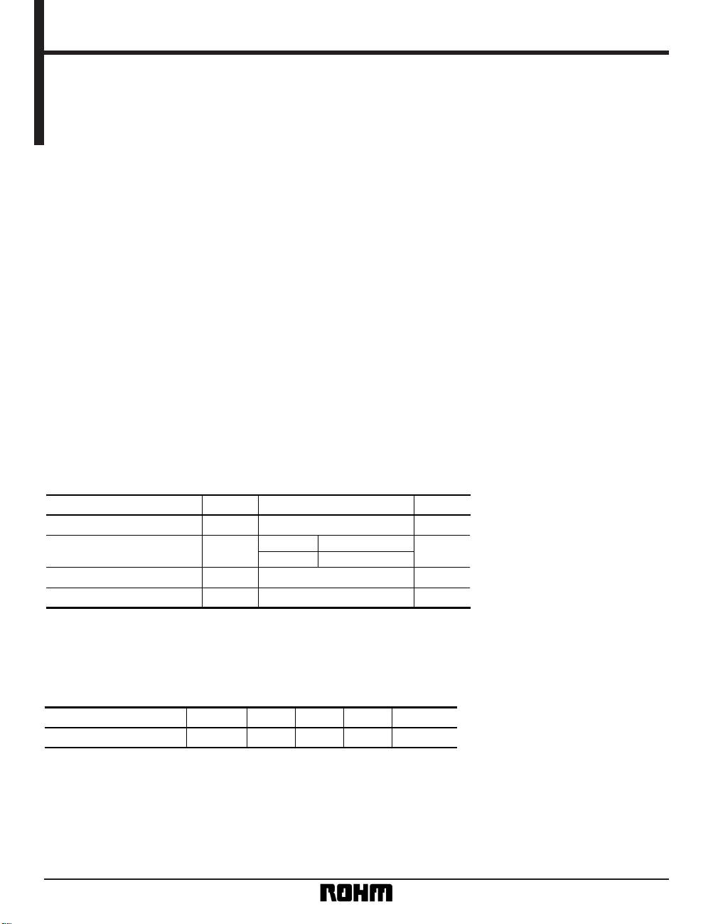
Block diagram
1 2 3 4 5 6 7 8 9 10 11
22 21 20 19 18 17 16 15 14 13 12
BUFF
BIAS
BIAS
BUFF
LOGIC
6dB
AMP
6dB
AMP
CONTROL
LOGIC
LATCHES
SHIFT
REGISTER
SW4
SW3
SW12
SW2
SW1
SW12
SW4
SW3SW2SW1
1 2 3 4 5 6 7 8 9 10 11 12 13 14
17 16 15
28 27 26 25 24 23 22 21 20 19 18
BUFF
BIAS
BUFF
BUFF
LOGIC
6dB
AMP
6dB
AMP
CONTROL
LOGIC
LATCHES
SHIFT
REGISTER
SW4
SW3
SW12
SW2
SW1
SW12
SW4
SW3
SW2
SW1
BA7630S
BA7630F
Page 3
3
Multimedia ICs BA7630S / BA7630F
•
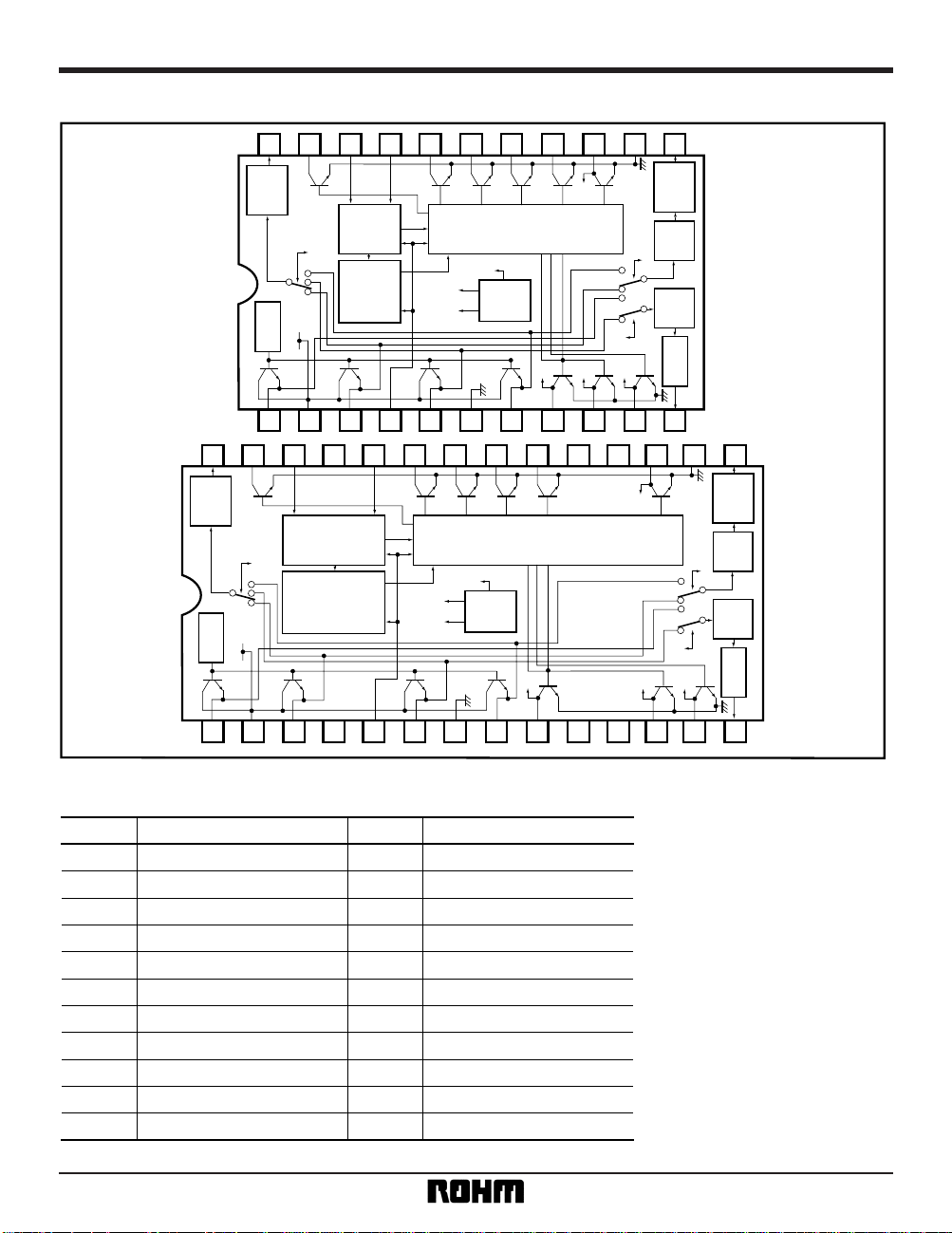
Electrical characteristics (unless otherwise noted Ta = 25°C and VCC = 5.0V)
Parameter
Symbol Min. Typ. Max. Unit Conditions
Measurement
Circuit
I
CC
——28 40 mA Fig.1
V
om
2.5 2.8 —
V
P-P
f = 1kHz, THD = 0.5%
Fig.1
G
V1
– 0.5 0 0.5 dB f = 1MHz, VIN = 1.0VP-P
GV2
5.5 6.0 6.5 dB f = 1MHz, VIN = 1.0VP-P
Gf
– 4.0 – 1.5 + 1.0 dB
10MHz / 1MHz
V
IN = 1.0VP-P
CTM
—– 60 – 45 dB
f = 4.43MHz
V
IN = 1.0P-P
VTH1 ~ 4
1.0 2.0 3.0 V
V
IH
3.0 —— —
—
V
Fig.3
V
IL
——1.0 V
I
IH
IIL
—
—
—210µA
Fig.2
– 80 – 100 – 150 —µA
I
QH1 ~ 4
150 230 350 µAVCC = 12V
I
QH5 ~ 9
— 050µAVCC = 12V
V
QL
— 0.1 0.5 V ICC = 2mA
Fig.1
f
Max.
250 500 ——kHz
t
su
——0.1 1.0 µs
Supply current
〈Analog〉
Maximum output level
Voltage gain 1
Voltage gain 2
Frequency characteristic
Interchannel crosstalk
〈Digital〉
"H" input voltage
"L" input voltage
"H" input current
"L" input current
"H" output leakage current 1
"H" output leakage current 2
"L" output voltage
Maximum clock frequency
Setup time
SW
1 ~ SW4 switch level
Page 4
4
Multimedia ICs BA7630S / BA7630F
•
Measurement circuits
BA7630S
22 21
20 1819 17 16 15 14 13
12
1 2
3 54 6 7 8 9 10
11
BUFF
BIAS
BUFF
BUFF
LOGIC
6dB
AMP
6dB
AMP
CONTROL
LOGIC
SHIFT
REGISTER
SW4
SW3
SW12
SW2
SW1
SW12
SW4
SW3SW2SW1
SWD SWE SWF
3V 1V
SW
G SWH SWI
LATCHES
V
21
1111
22222
~
1
50Ω
50Ω
50Ω
50Ω
~
SWC
2
1
~
SWB
2
1
~
SWA
OSC
1µ
47µ
V
CC5.0V
1µ 1µ 1µ
2
1
~
A
SWJ
V
2
1
~
SWK
V
2
1
~
Fig.1
Distortion
meter
Distortion
meter
Distortion
meter
+ + + +
Page 5

5
Multimedia ICs BA7630S / BA7630F
BA7630S
12
13
BUFF
BIAS
BUFF
BUFF
LOGIC
6dB
AMP
6dB
AMP
CONTROL
LOGIC
SHIFT
REGISTER
SW4
SW3
SW12
SW2SW1
SW12
SW4
SW3
SW2
SW1
SW0
A3
12V
V
1
LATCHES
V
A
14
15
16
17
18
19
20
21
22
11
10
9
8
7
6
5
4
3
2
1
Output
Measurement Circuit
Output
Measurement Circuit
Output
Measurement Circuit
SW1
A1
VCC
=
5.0V
A
2
5.0V
Input
Measurement
Circuit
Output
Measurement
Circuit
47
µ
V
A
Output
Measurement Circuit
Output
Measurement Circuit
Output
Measurement Circuit
Output
Measurement Circuit
Input
Measurement Circuit
Input
Measurement Circuit
Output
Measurement Circuit
Fig.2
+
Page 6

6
Multimedia ICs BA7630S / BA7630F
BA7630S
12
13
BUFF
BIAS
BUFF
BUFF
LOGIC
6dB
AMP
6dB
AMP
CONTROL
LOGIC
SHIFT
REGISTER
SW3
SW4
SW12
SW2SW1
SW12
SW4
SW3
SW2
SW1
SW1
SW2
SW3
CL
CL
CL
RL
RL
RL
12V
LATCHES
14
15
16
17
18
19
20
21
22
11
10
9
8
7
6
5
4
3
2
1
VCC
=
5.0V
47
µ
12V
PG
50Ω
PG
PG
50Ω
50Ω
RL
CL
SW9
RL
CL
SW8
RL
CL
SW7
RL
CL
SW6
RL
CL
SW5
RL
CL
SW4
Fig.3
+
Page 7

7
Multimedia ICs BA7630S / BA7630F
•
Measurement conditions
I
CC
22222222××× —
V
om1-1
V
om2-1
V
om3-1
2
2
2
1
2
2
2
1
2
2
2
1
1
1
2
1
2
×
×
×
×
×
×
×
×
×
×
×
×
×
2
2
2
V
om1-2
V
om3-2
2
2
1
2
2
2
2
1
×
×
×
×
2
2
×
×
×
×
2
2
×
×
Vom2-3
V
om4-3
2
1
2
2
1
2
2
2
×
×
×
×
×
×
1
2
2
2
×
×
×
×
Gv11-2
G
v13-2
G
v12-3
G
v14-3
2
2
2
1
1
2
2
2
2
2
1
2
2
1
2
2
×
×
×
×
×
×
×
×
1
2
×
×
×
×
1
2
×
×
2
2
1
2
×
×
×
×
×
×
Gv21-1
G
v22-1
G
v23-1
2
2
2
1
2
2
2
1
2
2
2
1
1
1
2
1
2
×
×
×
×
×
×
×
×
×
×
×
×
×
1
1
1
G
f
1-1
G
f
2-1
G
f
3-1
2
2
2
1
2
2
2
1
2
2
2
1
1
1
2
1
2
×
×
×
×
×
×
×
×
×
×
×
×
×
2
2
2
G
f
1-2
G
f
3-2
2
2
1
2
2
2
2
1
×
×
×
×
2
2
×
×
×
×
2
2
×
×
Gf2-3
G
f
4-3
2
1
2
2
1
2
2
2
×
×
×
×
×
×
1
2
2
2
×
×
×
×
CTM1-1-2
C
TM
1-1-3
C
TM
2-1-1
C
TM
2-1-3
C
TM
3-1-1
C
TM
3-1-2
2
2
2
2
2
2
2
2
1
2
1
2
1
2
2
2
2
1
2
1
2
1
2
2
1
1
1
1
2
2
1
1
2
2
2
2
×
×
×
×
×
×
×
×
×
×
×
×
×
×
×
×
×
×
×
×
×
×
×
×
1
1
1
1
1
1
C
TM
1-2-3
C
TM
3-2-122
2
1
2
2
1
2
×
×
×
×
1
2
×
×
×
×
1
1
×
×
CTM2-3-4
C
TM
4-3-212
2
2
2
1
2
2
×
×
×
×
×
×
1
2
1
1
×
×
×
×
SWASWBSWCSWDSWESWFSWGSWHSWISWJSW
K
Interchannel
crosstalk
Frequency
characteristics
Voltage gain 1
Voltage gain 2
Maximum
output level
Current
dissipation
Parameter
Measurement
method
Switch setting
Symbol
The measurements in the above table were made with switching voltage levels for SW1 to SW4 of "L" = 1V, and "H" = 3V.
Note 1: Connect distortion meters to the outputs. Adjust the input level so that the output distortion is 0.5% for a f = 1kHz sine wave input.
This output voltage is the maximum output level V
om (VP-P).
Note 2: Input a f = 1MHz, 1V
P-P sine wave. The voltage gain GV = 20 log VOUT / VIN (dB).
Note 3: Input a f = 1MHz and 10MHz, 1V
P-P sine wave. The frequency characteristic Gf = 20 log VOUT (f = 10M) / VOUT (f = 1M) (dB).
Note 4: Input a f = 4.43MHz, 1V
P-P sine wave.
0dB amplifier SW crosstalk is C
TM0, and the 6dB amplifier SW crosstalk is CTM6.
C
TM0 = 20 log VOUT / VIN (dB)
C
TM6 = 20 log VOUT / VIN + 6 (dB)
Note 1
Note 2
Note 3
Note 4
Page 8

8
Multimedia ICs BA7630S / BA7630F
•
Circuit operation
Digital block truth table
INPUT OUTPUT
Reset Clock Data SW
1
···························SW
9
H ××H····································H
LL
× SW
1-O
·····················SW
9-O
LH× SW
1-O
·····················SW
9-O
L ↑ HSW
1-O
·····················SW
9-O
L ↑ LSW
1-O
·····················SW
9-O
L ↓ LSW
1-O
·····················SW
9-O
L ↓ HSW
1-N
·····················SW
9-N
Data "L" sent to internal shift register
Data "H" sent to internal shift register
Internal shift register data unchanged
Contents of internal shift register sent to
internal latch
Note 1: H: high level
Note 2: L: low level
Note 3:
×: either H or L
Note 4: ↑: L to H transition
Note 5: ↓: H to L transition
Note 6: SW
1-O to SW9-O: SW1 to SW9 levels before establishing the input conditions shown in the table.
Note 7: SW
1-N to SW9-N
nearest clock ↓ transition.
Note
—
—
—
Analog truth table
(1) OUT1 switch
SW1SW
2
RESET SELECT
L L H IN1
L H H IN2
H L H IN3
H H H IN3
(2) OUT2 switch
SW
3
RESET SELECT
L H IN1
H H IN3
(3) OUT3 switch
SW
4
RESET SELECT
L H IN2
H H IN4
Note: When using the switches independently
without the digital block, the RESET pin
must be set to "H".
Page 9

9
Multimedia ICs BA7630S / BA7630F
1
CLK
DATA
2 3 4
5
At points 1 to 4 data is input to the shift register.
At point 5 the contents of the shift register are transferred to the
latch and simultaneously output.
Fig. 4 CLK and DATA relationship
•
Digital circuit operation
(1) Introduction
The BA7630S has 9-bit serial-to-parallel converter and
latch circuit that has been included to expand the number of microprocessor output ports. The breakdown
voltage of the output pins is 13V, so switch them in the
range 0 to 12V. In addition to controlling the BA7630S
switching block, these outputs can be used to control
audio switching, scrambling decoders, and television
sets.
(2) Using the serial-to-parallel convertor block
Signal input is basically done using clock and date
pulses. As shown in Fig.10, the date is read on the rising edge of the clock pulses. If the date is “H” on the
rising edge of the clock pulse, a “L” data bit is input to
the shift register, and if the data is “L” on the rising
edge of the clock pulse, a “H” data bit is input to the
shift register. The shift register is sequentially incremented by the bit corresponding to SW
1. Data in
excess of 9 bits is sequentially discarded.
If the data is “H” on a falling edge of the clock, the contents of the shift register are read into the internal latch,
and simultaneously output to the output port (the data
polarity is inverted on output). This output is maintained
until the latch is setup again.
To reset, set the RESET pin to “H”. The internal shift
register and latch contents go low (latch output all “H”),
for the duration that RESET is held high.
(3) Pulse timing
The pulse timing diagrams are given below.
123456789
—Q—Q—Q—Q—Q—Q—Q—Q—
Q
SW1 SW2 SW9
Reset
Latch
Latch
Data in
Data flow
Shift register
Fig. 5 Digital block
t
su
DATA
CLK
t
su
0.1µs (Typ.) 1.0µs (Max.)
Fig. 6 Clock rising edge and data relationship
(setup time)
t
su
DATA
CLK
t
su
0.1µs (Typ.) 1.0µs (Max.)
Fig. 7 Clock falling edge and data relationship
(setup time)
SW1 ~ SW
9
OUT
RESET
0.26µs (Typ.) 2.0µs (Max.)
t
PLHtPHL
Fig. 8 Reset and output relationship
(reset transmission time)
tPLH9 tPHL
SW1 ~ SW9
OUT
DATA
CLK
1.2µs (Typ.) 5.0µs (Max.)
Fig. 9 Clock falling edge and output relationship
(latch transmission time)
Page 10

10
Multimedia ICs BA7630S / BA7630F
•
Timing chart
RESET
DATA
CLOCK
SW
1
SW2
SW3
SW4
SW5
SW6
SW7
SW8
SW9
RESET RESETDATA DATA
Fig.10
Page 11

11
Multimedia ICs BA7630S / BA7630F
•
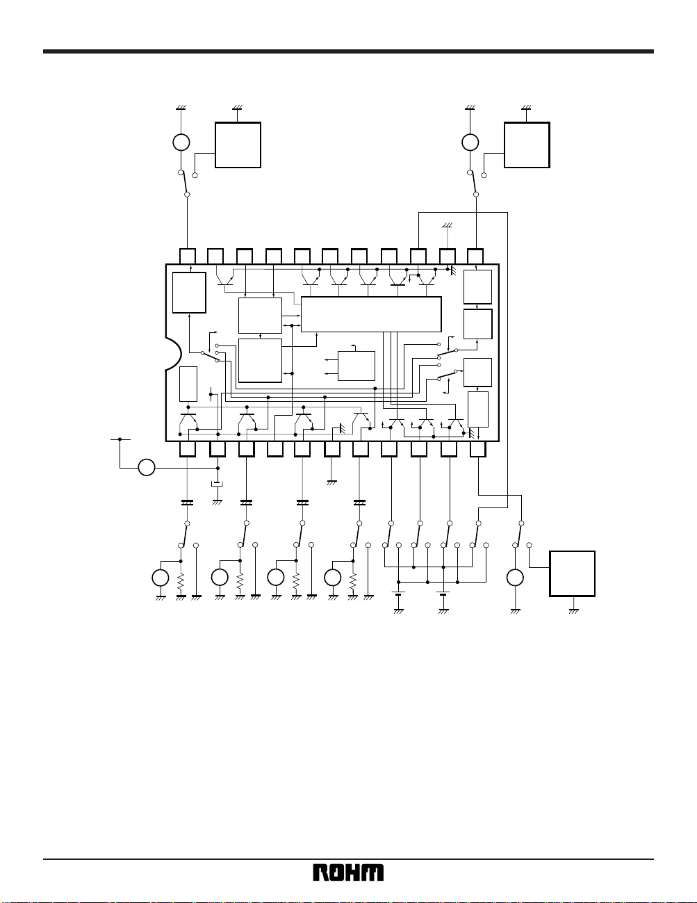
Application examples
(1) Analog block
BA7630S pin layout
75Ω
IN1
V
CC
VCC1
VCC2
to VCR
to
DECODER IN
to
TV IN
V
CC2
1µF
47µF
470 ~ 1000µF
470 ~ 1000µF
2SA933
2SA933
OUT1
OUT2
OUT3
GND
5V
R
R
75Ω
75Ω
from
VTR TUNER OUT
3 2
13
22
75Ω
IN2
1µF
from
DECODER OUT
5
75Ω
IN3
1µF
from
TV OUT
7
75Ω
IN4
1µF
from
VIDEO OUT
1
GND
6
12
11
6dB
AMP
6dB
AMP
V
CC2
R
5V 100
12V 390
Fig.11
++
+
++
+
+
+
(2) Digital block
SW OUT
VCC 4.5 ~ 13V
SW
1 ~ SW9
SW1 ~ SW4
ONLY
OPEN
COLLECTOR
22k
50kΩ
28kΩ
Fig.12
Page 12

12
Multimedia ICs BA7630S / BA7630F
•
Electrical characteristic curves
0
– 2
– 4
– 6
– 8
– 10
– 12
– 14
– 16
– 18
– 20
100k 200k 500k
FREQUENCY (Hz)
GAIN (dB)
1M 2M 5M 10M20M30M
3pin-22pin
5pin-22pin
7pin-22pin
V
IN
=
10VP-P
Fig. 13 Frequency characteristic(OUT1)
0
– 20
– 30
– 40
– 50
– 10
– 60
– 70
100k 200k 500k
FREQUENCY (Hz)
CROSSTALK: CT (dB)
1M 2M 5M 10M 20M
3pin-22pin
5pin-22pin
7pin-22pin
V
IN = 1.0VP-P
Fig. 14 Crosstalk characteristic (OUT1)
6
4
2
0
– 2
– 4
– 6
– 8
– 10
– 12
– 14
100k 200k 500k
FREQUENCY (Hz)
GAIN (dB)
1M 2M 5M 10M 20M30M
1pin-11pin
5pin-11pin
3pin-12pin
7pin-12pin
Input 1V
P-P
Fig. 15 Frequency characteristic
(OUT2 and OUT3)
0
– 20
– 30
– 40
– 50
– 10
– 60
– 70
100k 200k 500k
FREQUENCY (Hz)
CROSSTALK: CT (dB)
1M 2M 5M 10M 20M
1pin-11pin
5pin-11pin
3pin-12pin
7pin-12pin
Input 1V
P-P
Fig. 16 Crosstalk characteristic
(OUT2 and OUT3)
•
External dimensions (Units: mm)
BA7630S BA7630F
SDIP22 SOP28
3.95 ± 0.3
0.51Min.
19.4 ± 0.3
3.4 ± 0.2
0.5 ± 0.1
6.5 ± 0.3
1
11
1222
0.3
± 0.1
0° ~ 15°
1.778
7.62
0.15
28 15
141
0.4 ± 0.1
0.3Min.
0.15 ± 0.1
7.5 ± 0.2
9.9 ± 0.3
18.5 ± 0.2
0.11
2.2 ± 0.1
1.27
 Loading...