

Page 1
1
Multimedia ICs
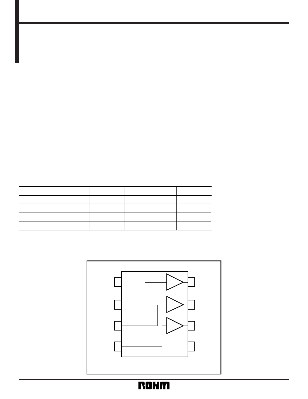
75Ω driver IC with 3 internal circuits
BA7623F
The BA7623F is a 75Ω driver-IC developed for use in video equipment. Since the input is coming directly with no
bias at the base pin, the DC potential for the previous stage can be used for direct DC coupling. Each output can
drive two loads (75Ω×2).
•
Applications
Video cassette recorders, televisions and camcorders
•
Block diagram
GND
IN1
IN2
IN3
OUT1
OUT2
OUT3
V
CC
1
2
3
4
8
7
6
5
75Ω
driver
75Ω
driver
75Ω
driver
•
Features
1) Can be directly coupled to the previous circuit.
2) Each output can drive two loads.
•
Absolute maximum ratings (Ta = 25°C)
Parameter
Symbol Limits Unit
V
CC
8.0 V
Pd 550
∗
mW
Topr – 25 ~ + 75 °C
Tstg – 55 ~ + 125 °C
∗
Reduced by 5.5mW for each increase in Ta of 1°C over 25°C.
Power supply voltage
Power dissipation
Operating temperature
Storage temperature
Page 2
2
Multimedia ICs BA7623F
•
Pin descriptions
1 GND
2 IN1
3 IN2
4 IN3
5
6 OUT3
7 OUT2
8 OUT1
V
CC
Pin No.
Ground connection
Direct-coupling input
Input composite video or component video (RGB) signals.
Keep the input signal level in the range 0.5V to 3.8V.
Direct-coupling input
Input composite video or component video (RGB) signals.
Keep the input signal level in the range 0.5V to 3.8V.
Direct-coupling input
Input composite video or component video (RGB) signals.
Keep the input signal level in the range 0.5V to 3.8V.
FunctionPin name
Power supply
Direct-coupling output
Output for the signal input to IN3. When connected to earth a protection circuit operates,
and the IC enters power-save mode.
Direct-coupling output
Output for the signal input to IN2. When connected to earth a protection circuit operates,
and the IC enters power-save mode.
Direct-coupling output
Output for the signal input to IN1. When connected to earth a protection circuit operates,
and the IC enters power-save mode.
•
Electrical characteristics (unless otherwise noted, Ta = 25°C and VCC = 5V, and load is two system drive)
Parameter
Symbol Min. Typ. Max. Unit
Conditions
4.5 5.0 5.5 V
— 25.2 37.8 mA
V
om 2.9 3.4 — V
P-P
– 1.0 – 0.5 0 dB
Cf – 3 0 1 dB
DG1 — 0.4 1.0 %
DP1 — 0.4 1.0
DG2 — 0.7 2.0 %
DP2 — 0.7 2.0
C
T — – 60 — dB
T
HD — 0.1 0.5 %
V
CC
I
CC
G
V
deg
deg
Operating voltage
Supply current
Maximum output level
Voltage gain
Frequency characteristic
Differential gain 75Ω drive 1
Differential phase 75Ω drive 1
Differential gain 75Ω drive 2
Differential phase 75Ω drive 2
Interchannel crosstalk
Total harmonic distortion
V
IN = 2.0VP-P, standard staircase signal
V
IN = 2.0VP-P, standard staircase signal
V
IN = 2.0VP-P, standard staircase signal
V
IN = 2.0VP-P, standard staircase signal
No signal
f = 1kHz, THD = 1.0%
f = 1MHz, V
IN = 2.0VP-P
f = 4.43MHz, VIN = 2.0VP-P
f = 1kHz, VIN = 1.0VP-P
10MHz / 1MHz, VIN = 1.0VP-P
—
Page 3

3
Multimedia ICs BA7623F
•
Input / output circuits
2, 3, 4
pin
IN1, 2, 3
VCC
20k
6, 7, 8
pin
OUT1, 2, 3
VCC
•
Measurement circuit
123
SWD
123
SWE
123
SWF
Vector
Scope
Analyzer
Audio
Vector
Scope
Analyzer
Audio
Vector
Scope
Analyzer
Audio
V
~
V
~
V
~
75
470µ
+
75
75
470µ
+
75
75
470µ
75
SWA SWB SWC
75
1000µ
+
75
75
75
1
2
3
4
8
7
6
5
75Ω
driver
75Ω
driver
75Ω
driver
V
CC = 5V
0.022µF
47µF
+
~ ~
OSC
SG
2.1V 2.1V 2.1V
600
1µ 1µ 1µ
1k 1k 1k
123
+
+
+ +
Fig. 1
The circuit for driving one 75Ω output load.
The circuit for driving two 75Ω output loads is as
~ ~
OSC
SG
2.1V 2.1V 2.1V
600
1µ 1µ 1µ
1k 1k 1k
123
+
+ +
~ ~
OSC
SG
2.1V 2.1V 2.1V
600
1µ 1µ 1µ
1k 1k 1k
123
+
+ +
Page 4

4
Multimedia ICs BA7623F
•
Measurement conditions
IN1 IN2 IN3 OUT1 OUT2 OUT3
SWA SWB SWC SWD SWE SWF
I
cc 333××× —
—
—
—
—
V
om12 1333××
Vom22 313× 3 ×
Vom32 331××3
G
v12 1333××
Gv22 313× 3 ×
Gv32 331××3
f12 1333
××
f22 3 1 3 × 3 ×
f32 3 3 1 ××3
C
T112 1 3 3 × 3 ×
CT113 1 3 3 ××3
C
T211 3133××
CT213 3 1 3 ××3
C
T311 3313××
CT312 3 3 1 × 3 ×
THD12 1333××
THD22 313× 3 ×
THD32 331××3
DG1 2331
××
DG2 323× 1 ×
DG3 332××1
DP1 2331
××
DP2 3 2 3 × 1 ×
DP3 3 3 2 ××1
∗
1
∗
2
∗
3
Symbol Conditions
Current dissipation
Maximum output level
Voltage gain
Frequency characteristic
Interchannel crosstalk
Total-harmonic distortion
Differential gain (DG)
Differential phase (DP)
×: Any of switches 1, 2, or 3 possible.
∗
1: Connect a distortion meter to the output, and input a f = 1kHz sine wave. Adjust the input level until the output distortion is 1.0%. This output voltage
at this time is the maximum output level Vom (VP-P).
∗
2: Input a 2.0V
P-P, 1MHz sine wave. The voltage gain is given by GV = 20 log (VOUT / VIN)(dB).
∗
3: Input a 1.0V
P-P, 1kHz sine wave. Connect a distortion meter to the output and measure the total-harmonic distortion.
Parameter
Page 5

5
Multimedia ICs BA7623F
•
Application example
1
2
3
4
8
7
6
5
75Ω
driver
75Ω
driver
75Ω
driver
47µF
0.022µF
VCC = 5V
75
1000µ
+
+
VIDEO
OUT1
75
VIDEO
OUT2
75
1000µ
+
VIDEO
OUT3
75
VIDEO
OUT4
75
1000µ
+
VIDEO
OUT5
75
VIDEO
OUT6
R1
Q1
GND
R1
Q1
R1
Q1
Fig. 2
Page 6

6
Multimedia ICs BA7623F
•
Electrical characteristic curves
GAIN: GV (dB)
FREQUENCY: f (Hz)
20
0
– 20
– 40
100k 1M 10M 100M
20
0
20
40
100k 1M 10M 100M
Fig. 3 Frequency characteristic
GAIN: GV (dB)
FREQUENCY: f (Hz)
0
– 20
– 40
– 60
– 80
100k 10M 100M1M
Fig. 4 Crosstalk
•
External dimensions (Units: mm)
SOP8
0.4 ± 0.11.27
0.15
0.3Min.
0.15 ± 0.1
0.11
6.2 ± 0.3
4.4 ± 0.2
5.0 ± 0.2
85
41
1.5 ± 0.1
•
Operation notes
(1) The input signals are signals such as composite video signals, or component video (RGB) signals.
(2) When using direct coupling, keep the input signals in the range: 0.5V to 3.8V.
 Loading...