

Page 1
1
Multimedia ICs
75Ω driver IC with 3 internal circuits
BA7622F
The BA7622F is a 75Ω driver-IC developed for use in video equipment. It includes three 75Ω driver circuis,two of
which have sync-tip clamp inputs.The other driver has a biased input terminated with a 20kΩ resistor.Each output
can drive two loads (75Ω × 2).
•
Applications
Video cassette recorders, televisions and camcorders
•
Features
1) Two built-in clamp circuits.
2) Simultaneous drive of Y, C and composite video signals possible.
3) Each output can drive two loads.
•
Absolute maximum ratings (Ta = 25°C)
Parameter
Symbol Limits Unit
8.0 V
Pd mW
Topr °C
Tstg °C
550
∗
V
CC
– 25 ~ + 75
– 55 ~ + 125
Power supply voltage
Power dissipation
Operating temperature
Storage temperature
∗
Reduced by 5.5mW for each increase in Ta of 1°C over 25°C.
Page 2
2
Multimedia ICs BA7622F
•
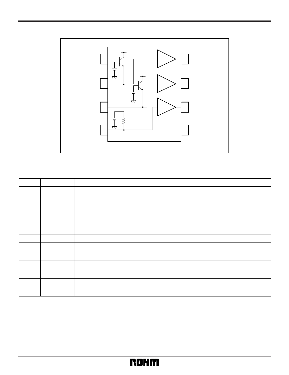
Pin descriptions
1 GND
2 IN1
3 IN2
4 IN3
5
6 OUT3
7 OUT2
8 OUT1
Pin No.
V
CC
Ground connection
Clamp input
Input composite video or the Y signal separated from Y / C.
Clamp input
Input composite video or the Y signal separated from Y / C.
Biased input
Input the chroma signal. Terminated with a 20kΩ resistor.
Power supply
Biased output
Output for the signal input to IN3. When connected to earth a protection circuit operates,
and the IC enters power-save mode.
Clamped output
Output for the signal input to IN2. When connected to earth a protection circuit operates,
and the IC enters power-save mode.
Clamped output
Output for the signal input to IN1. When connected to earth a protection circuit operates,
and the IC enters power-save mode.
Pin name Function
•
Block diagram
GND
IN1
IN2
IN3
OUT1
OUT2
OUT3
VCC
NO Clamp
Clamp
Clamp
20k
1
2
3
4
8
7
6
5
75Ω
driver
75Ω
driver
75Ω
driver
Page 3
3
Multimedia ICs BA7622F
•
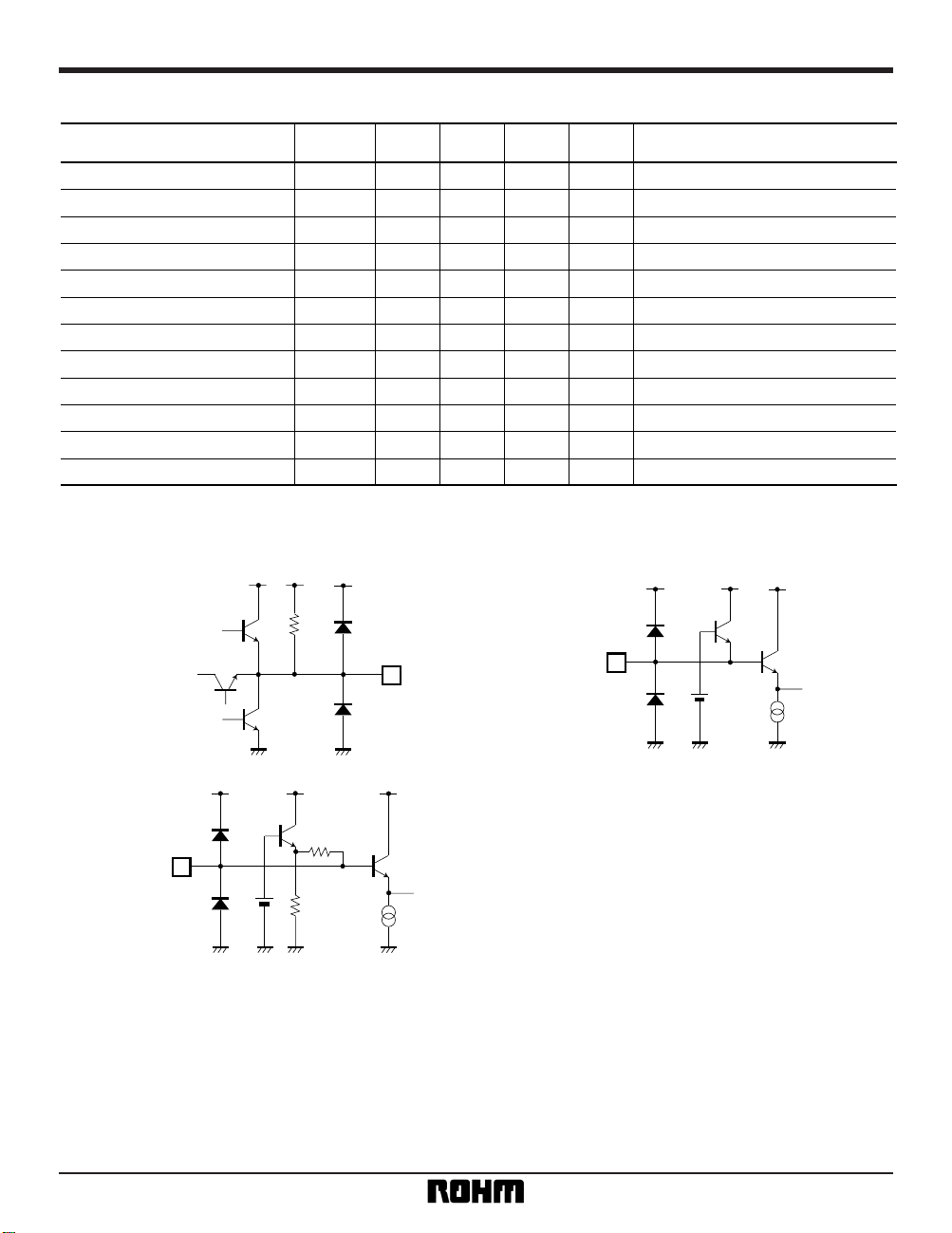
Electrical characteristics (unless otherwise noted, Ta = 25°C and VCC = 5V, and load is two system drive)
Parameter
Symbol Min. Typ. Max. Unit
Conditions
4.5 5.0 5.5 V
—mA
V
om —
—
—
Gv 0 dB
Gf – 3 0 dB
DG1 — 0.4 1.0 %
DP1 — 0.4 1.0
DG2 — 0.7 2.0 %
DP2 — 0.7 2.0
C
T — – 60 — dB
— 0.1 0.5 %
ZIN3 17 20 23
2.8
– 1.2
23.6
3.3
– 0.6
35.4
1.3
deg
deg
V
CC
I
CC
V
P-P
kΩ
T
HD32
Operating voltage
Circuit current
Maximum output level
Voltage gain
Frequency characteristics
Differential gain 75Ω drive 1
Differential phase 75Ω drive 1
Differential gain 75Ω drive 2
Differential phase 75Ω drive 2
Interchannel crosstalk
Input impedance (VIN3)
Total-harmonic distortion (VIN3)
No signal
f = 1kHz, THD = 1.0%
f = 1MHz, V
IN = 2.0VP-P
10MHz / 1MHz, VIN = 1.0VP-P
VIN = 2.0VP-P, standard staircase signal
V
IN = 2.0VP-P, standard staircase signal
V
IN = 2.0VP-P, standard staircase signal
V
IN = 2.0VP-P, standard staircase signal
f = 4.43MHz, V
IN = 2.0VP-P
f = 1kHz, VIN = 1.0VP-P
•
Input / output circuits
VCC
20k
6, 7, 8
OUT1, 2, 3
VCC
100µA
IN1, 2
2, 3
VCC
100µA
IN3
4
20k
10k
Page 4

4
Multimedia ICs BA7622F
•
Measurement circuit
123
4
SWC
V
CC = 5V
V
~~
OSC
SG
600
1µ 1µ1µ
200µA50µA
75
1000µ
+
75
75
75
OSC
SG
OSC
SG
V
~
600
1µ 1µ
1µ
4
V
CC = 5V
V
~~
600
1µ 1µ1µ
123
4
SWA
~
123
SWB
200
µA
V
CC = 5V
1
75Ω
driver
2
3
4
75Ω
driver
75Ω
driver
Clamp
Clamp
20k
NO Clamp
5
75
470µ
+
75
6
75
470µ
+
75
7
75
470µ
+
75
8
0.022µF
47µF
Analyzer
Audio
123
SWF
Vector
Scope
23
Analyzer
Audio
123
SWD
1
SWE
Vector
Scope
Analyzer
Audio
Vector
Scope
V
~
V
~
V
~
VCC = 5V
+
+++++++++
Fig.1
The circuit for driving one 75Ω output load.
The circuit for driving two 75Ω output loads is as.
Page 5

5
Multimedia ICs BA7622F
•
Measurement conditions
IN1 IN2 IN3 OUT1 OUT2 OUT3
SWA SWB SWC SWD SWE SWF
333××× —
—
—
V
om12 1333××
∗
1Vom22 313× 3 ×
V
om32 331××3
G
v12 1333××
∗
2Gv22 313× 3 ×
G
v32 331××3
f12 1333××
f22 3 1 3 × 3 ×
f32 3 3 1 ××3
C
T112 1 3 3 × 3 ×
C
T113 1 3 3 ××3
C
T211 3133××
C
T213 3 1 3 ××3
C
T311 3313××
C
T312 3 3 1 × 3 ×
T
HD12 1333××
∗
4THD22 313× 3 ×
T
HD32 331××3
ZIN3 3 3 4
× × ×
∗
3
I
CC
Parameter Symbol Conditions
∗
1: Connect a distortion meter to the output, and input a f = 1kHz sine wave. Adjust the input level until the output distortion is 0.5%. This output voltage
at this time is the maximum output level V
om (VP-P).
∗
2: Input a 2.0VP-P, 1MHz sine wave. The voltage gain is given by GV = 20 log (VOUT / VIN).
∗
3: Measure the input pin voltage VIN50 when a current of DC50µA is flowing into the input pin. Measure the input pin open-circuit voltage VIN0.
The input impedance is given by Z = (V
IN50 - VIN0) / 50∗10
-6
[Ω].
∗
4: Input a 1.0VP-P, 1kHz sine wave. Connect a distortion meter to the output and measure the total-harmonic distortion.
Current dissipation
Maximum output level
Voltage gain
Frequency characteristic
Interchannel crosstalk
Total-harmonic distortion
Input resistance
×
: Any of switches 1, 2, or 3 possible.
Page 6

6
Multimedia ICs BA7622F
•
Application example
VCC = 5V
47µF 0.022µF
75
VIDEO
OUT1
75
1
2
3
4
8
7
6
5
75Ω
driver
75Ω
driver
75Ω
driver
Clamp
Clamp
1µF
20k
NO Clamp
1µF
0.01µF
Composite
Video
Signal
Y Signal
C Signal
1000µF
+
1000µF
+
1µF
+
YC
YC
75
75
75
75
VIDEO
OUT2
+
+
+
Fig.2
•
Electrical characteristic curves
GAIN: GV (dB)
FREQUENCY: f (Hz)
20
0
– 20
–40
100k 1M 10M 100M
Fig. 3 Frequency characteristic
GAIN: GV (dB)
FREQUENCY: f (Hz)
0
–20
– 40
–60
–80
100k 10M 100M1M
Fig. 4 Crosstalk
Page 7

7
Multimedia ICs BA7622F
•
Extermal dimensions (Units: mm)
SOP8
0.4 ± 0.11.27
0.15
0.3Min.
0.15 ± 0.1
0.11
6.2 ± 0.3
4.4 ± 0.2
5.0 ± 0.2
85
41
1.5 ± 0.1
 Loading...