

Page 1

BA6780 / BA6780FP-Y
Optical disc ICs
2-channel driver for CD changers
BA6780 / BA6780FP-Y
The BA6780 and BA678 0FP-Y are 2-channel driver IC for CD chan gers that inculdes a reversible, variable s peed
electronic governor and a reversible driver. On sets that have dual-rail power supplies, the BA6780 and BA6780FP-Y can
be operated from just the negative supply to reduce influence on the positive power supply.
The input uses PW M control, and it is poss ible to directly input from a microprocessor running off the positi ve power
supply.
zApplications
Changers for CD players and MD players.
zFeatures
1) Output voltage can be freely set using the output voltage setting pin.
2) Internal mute function if the power supply voltage drops.
3) Thermal shutdown function. (Contains hysteresis)
4) PWM input.
5) Settable reference voltage output pin.
6) Wide operating supply voltage.
z
zAbsolute maximum ratings (T a = 25°C)
zz
Parameter Symbol Limits Unit
FIN, VRIN
V
Pd
CC
CC
IN
Power supply voltage V
Logic input voltage
Power dissipation
Maximum current consumption Imax 1.4 A
Operating temperature Topr −25∼+75 ˚C
Storage temperature Tstg −55∼+150 ˚C
∗1 When a DIP18 package is used.Reduced by 10.48mW for each increase inTa of 1˚C over 25˚C.
∗2 When mounted on a PCB board (70mm×70mm, t=1.6mm glass epoxy board).
Reduced by 11.6mW for each increase in Ta of 1˚C over 25˚C.
∗3 Should not exceed Pd or ASO values.
z
zRecommended operating conditions (T a = 25°C)
zz
Parameter Symbol Limits Unit
Power supply voltage V
Input voltage for Vin V
BA6780
BA6780FP-Y
18 V
22 V
∗1
1.31
∗2
1.45
∗3
7∼16 V
0∼V
CC
/ 2−1.0 V
W
Page 2
Optical disc ICs
z
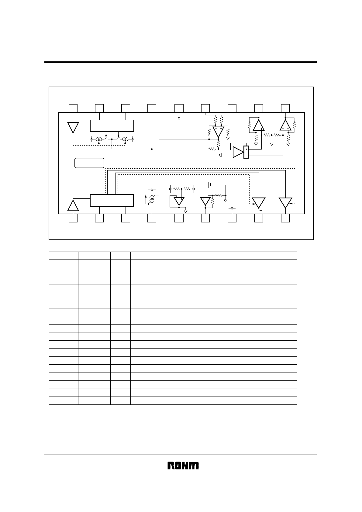
zBlock diagram and pin descriptions
zz
BA6780
BA6780 / BA6780FP-Y
VIN2 FIN2 RIN2 Cτ2 FBIN−V
18 17
V
IN
1/2
1 2
FWD/REV CONTROLLER
CC
V
THERMAL
SHUT DOWN
REVERSIBLE DRIVER
FWD/REV CONTROLLER
V
IN
16
GOVERNOR DRIVER
3
15 14 13 12 11 10
EE
V
V
EE
OUT
I
4 5 6 7 8 9
EE
V
EE
DETECTOR
40k40k
CC
V
Vref
10k
10k
10k
Vref
V
EE
20k
17.1k
Vconst
VregVrefIoutRIN1FIN1VIN1
Pin No. Pin name I/O Function
IN
1V
1 I Input pin for setting high output voltage for the reversible driver
2 FIN1 I Input pin for forward control signal for the reversible driver
3 RIN1 Input pin for reverse control signal for the reversible driver
I
4 Iout O Governor load current detector output (open collector )
5 Vref O Internal reference voltage pin
6 Vreg O 4.6V constant voltage output
7VCCI Power supply (+)
8 OUT1+ Reversible driver output (+)
O
9 OUT1− O Reversible driver output (−)
10 OUT2− O Governor output (−)
11 OUT2+ O Governor output (+)
12 FBIN+ I Governor load current detector amplifier input (+)
13 FBIN− Governor load current detector amplifier input (−)
14 V
EE
I
I Power supply (−) (connection within substrate)
15 Cτ 2 I For connection of capacitor for the governor PWM filter
16 RIN2 I Governor reverse control signal input
17 FIN2 I Governor forward control signal input
IN
18 V
1 Refer to operating notes.
∗
2 Input pin for setting high output voltage for the governor
I
FBIN+ OUT2+ OUT2−
3.2k
10k
10k
10k
Vref
V / I
V
EE
V
CC
CC
∗1
10k
Vref
DRIVE BUFFER
10k
Vref
DRIVE BUFFER
10k
10k
10k
Vref
OUT1−OUT1+V
Page 3
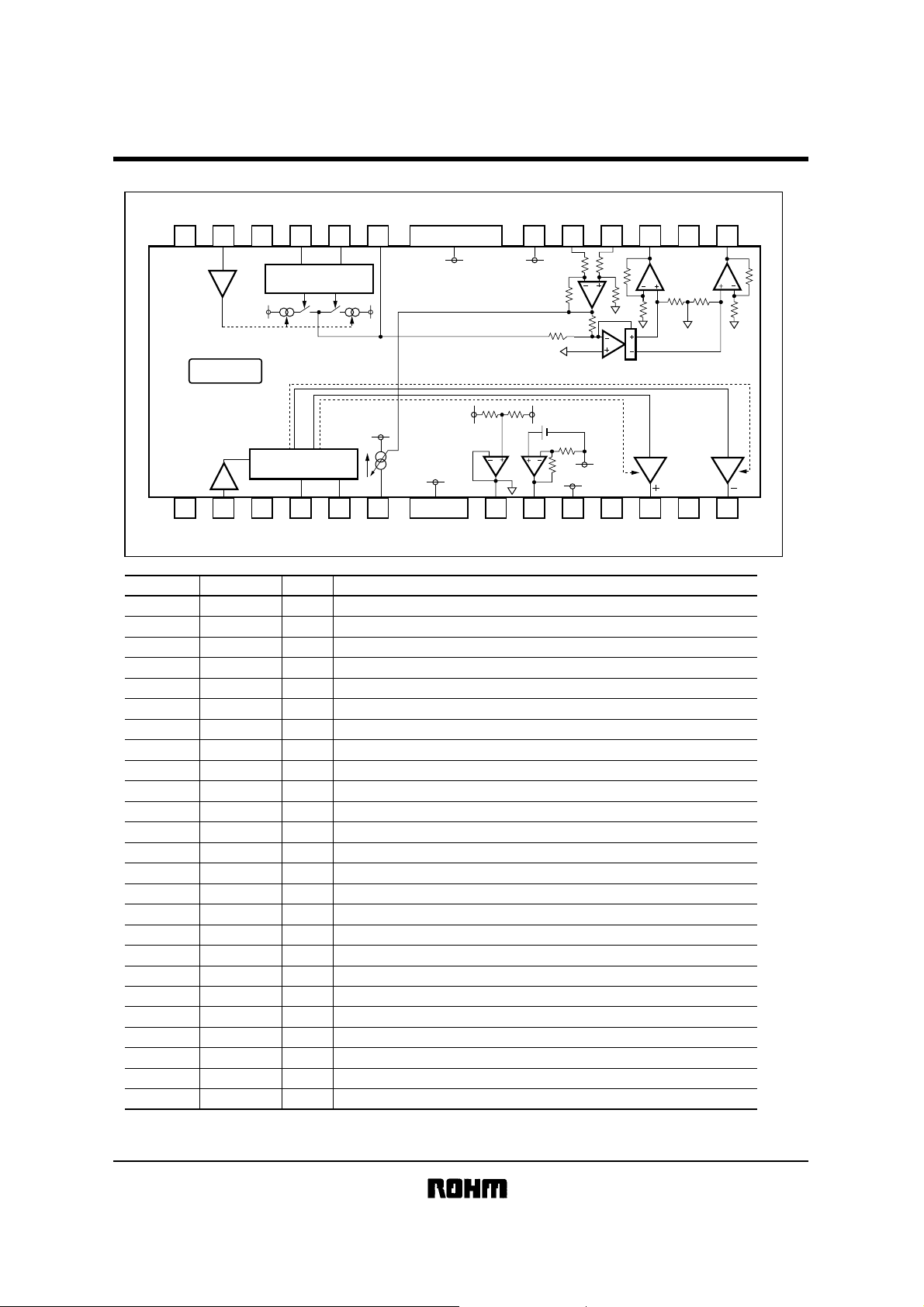
Optical disc ICs
BA6780FP-Y
BA6780 / BA6780FP-Y
VIN2 FIN2 RIN2 Cτ2 FBIN−V
25
THERMAL
SHUT DOWN
1
1/2
V
IN
V
IN
22 21 20 19
2324
GOVERNOR DRIVER
FWD/REV CONTROLLER
CC
V
REVERSIBLE DRIVER
FWD/REV CONTROLLER
4 5 6 87
32
EE
V
V
EE
V
I
OUT
EE
V
EE
CC
V
40k40k
Vref
Pin No. Pin name I/O Function
1 N.C. −
IN
2V
1 I
3 N.C
4 FIN1 I
5 RIN1 I
6 Iout O
7 Vref O
8 Vreg
9V
CC
Input pin for setting high output voltage for the reversible driver
−
Input pin for forward control signal for the reversible driver
Input pin for reverse control signal for the reversible driver
Governor load current detector output (open collector )
Internal reference voltage pin
4.6V constant voltage output
O
I
Power supply (+)
10 N.C. −
11 OUT1+ O
Reversible driver output (+)
12 N.C. −
13 OUT1−
14 OUT2− O
Reversible driver output (−)
O
Governor output (−)
15 N.C. −
16 OUT2+ O
17 FB IN + I
18 FB IN −
19 V
EE
20 Cτ 2
21 R IN 2 I
22 F IN 2 I
Governor output (+)
Governor load current detector amplifier input (+)
Governor load current detector amplifier input (−)
I
I
Power supply (−) (connection within substrate)
I
For connection of capacitor for the governor PWM filter
Governor reverse control signal input
Governor forward control signal input
23 N.C. −
24 VIN2I
25 N.C.
1 Refer to operating notes.
∗
Input pin for setting high output voltage for the governor
−
V
VregVrefIoutRIN1FIN1VIN1
EE
EE
V
Vconst
FBIN+ OUT2+ OUT2−
16 15 1418
17
10k
10k
20k
17.1k
10k
Vref
3.2k
V
EE
V
CC
10
CC
∗1
10k
10k
Vref
EE
10k
10k
Vref
DRIVE BUFFER
10k
Vref
DRIVE BUFFER
11 12 139
10k
10k
10k
Vref
OUT1−OUT1+V
Page 4
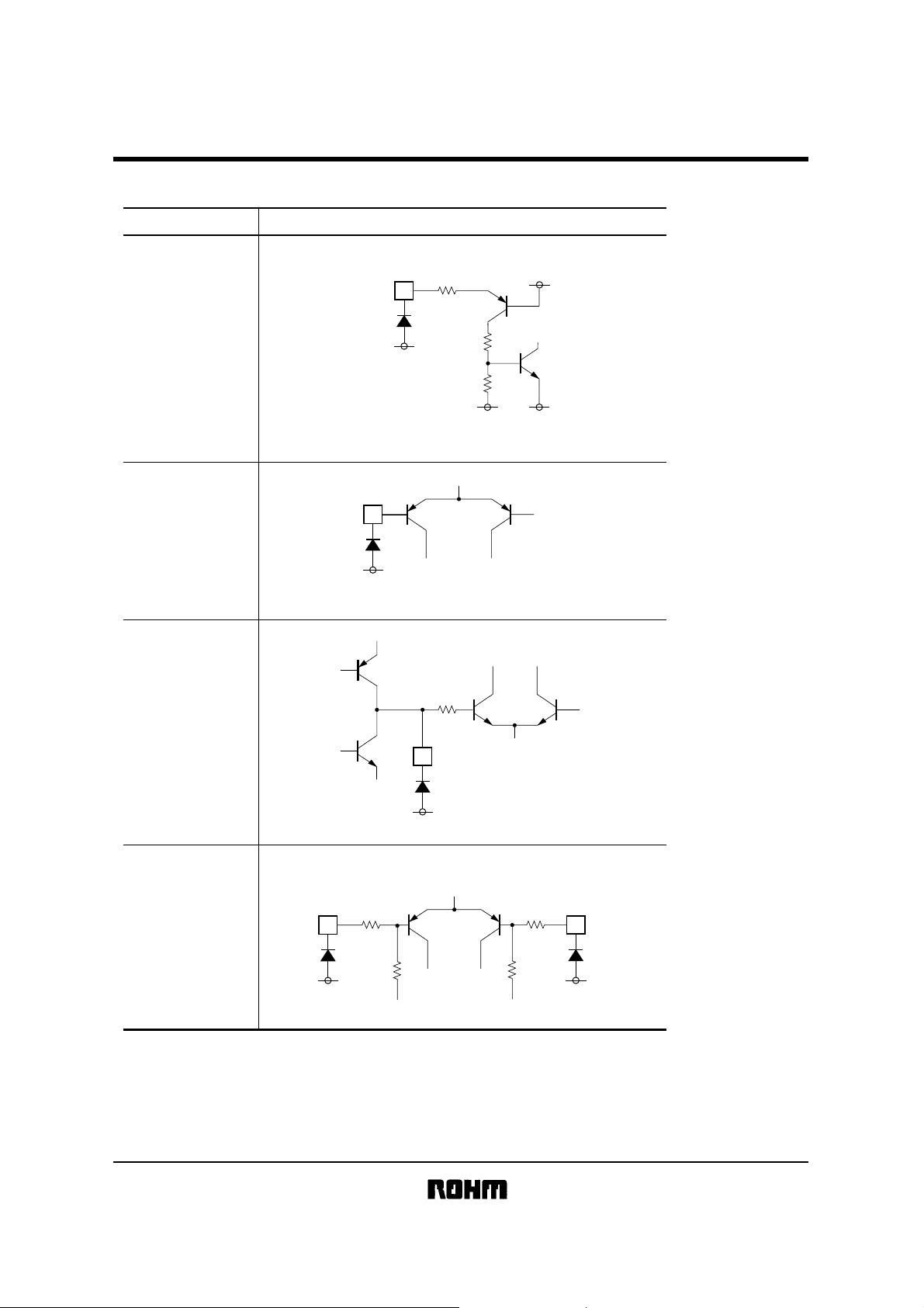
Optical disc ICs
z
zInput / output circuits ( ( ) :pins f or BA6780FP-Y )
zz
Pin function Equivalent circuit
pin 2, 3, 16, 17
( pin4, 5, 21, 22 )
85k
BA6780 / BA6780FP-Y
V
CC
Logic input
Voltage setting input
For connection of
capacitor for PWM
filter
pin1, 18
( pin2, 24 )
24k
V
EE
24k
V
V
EE
V
EE
10k
pin15
( pin20 )
EE
Load current detector
pin13
( pin18 )
V
EE
10k
10k
V
EE
10k
10k
V
EE
pin12
( pin17 )
Page 5
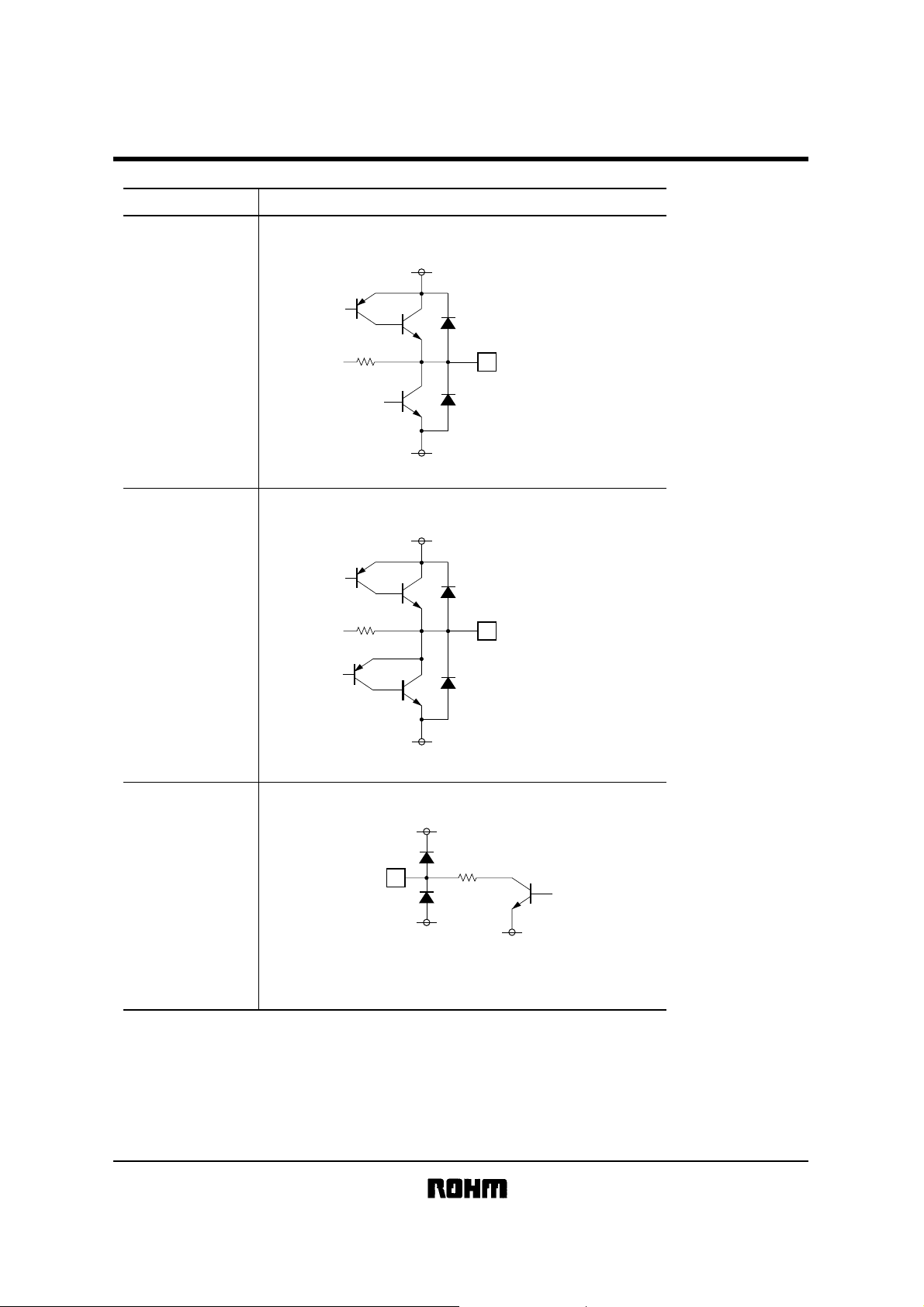
Optical disc ICs
Pin function Equivalent circuit
V
CC
BA6780 / BA6780FP-Y
Output
(reversible driver)
Output
(governor)
10k
10k
pin8, 9
( pin11, 13 )
V
EE
V
CC
pin10, 11
( pin14, 16 )
V
EE
Load current detector
signal output
(governor)
pin4
( pin6 )
V
CC
1k
V
EE
V
EE
Page 6

BA6780 / BA6780FP-Y
Optical disc ICs
z
zElectrical characteristics (unless otherwise noted, T a = 25°C, VCC = 10V) ( ∗1 BA6780FP-Y)
zz
Parameter
Quiescent current
Mute on voltage
Mute off voltage
Vref input voltage range
Vref pin current
PWM input high level voltage
PWM input low level voltage
PWM input high level current
PWM input low level current
Symbol Min. Typ. Max. Unit
Q
I
V
CC1
V
CC2
V
IN
I
V
V
IH
I
IL
I
<Electronic governor>
Output offset voltage
Max. pin-to-pin output voltage
Pin-to-pin output voltage 1-1
Pin-to-pin output voltage 1-2
Pin-to-pin output voltage 1-3
Pin-to-pin output voltage 1-4
Voltage gain of positive feedback amplifier
V
V
V
V
OF
V
OM
OUT11
OUR12
OUT13
OUT14
G
VNF
<Reversible driver>
Output saturation voltage
Pin-to-pin output voltage 2-1
Pin-to-pin output voltage 2-2
Pin-to-pin output voltage 2-3
Pin-to-pin output voltage 2-4
Output load fluctuation
V
V
V
V
V
CESAT
OUT21
OUT22
OUT23
OUT24
V
OUT
−
8.0 16.0 mA
−
5.5 − V
IN
0 −
−
IH
IL
4.0
− 1.0 V
−
−1.0 1.0 µA
−100
6.0
−
−
0.02
−
−
−
−
0
6.5
4.2 4.7 5.2
−5.2 −4.7 −4.2
−100
0 100 mV
−50 0 50
20.5 22.0 23.5
−
1.0 2.1
4.5
5.0 5.5
−5.5 −5.0 −4.5
−50 0 50
−50 0 50
− 200
3.5
V
4V
1.0
100
100
µA
−
V
µA
mV
−
V
V
V
mVV
dB
V
V
V
mV
mV
400
mV
Conditions
Open mode with no load
CC
Mute on voltage when V
falls
Mute off voltage when VCC rises
−
−
With V
CC
as the reference potential
With VCC as the reference potential
−
−
RL (load)=9Ω, RO (current detector)=0.6Ω
L
(load)=9Ω, RO (current detector)=0.6Ω
R
Forward mode
Reverse mode
Brake mode
Stop mode
ref
=
0V, VIN=−
V
I
O
=
100mA, V
12, 13 open
17, 18pin open ∗
RL (load)=9
Ω
RO (current detector)=0.6Ω
V
IN
2=2.5V
20dBV, f=1kHz
IN
2
=
5V, Total of upper side
1
and lower side ineffective voltage of output Tr
Forward mode
Reverse mode
Brake mode
Stop mode
O
I
=
100mA
IN
1
=
2.5V
V
Difference in output voltage for
I
O
=
400mA and
IO=
100mA
<4.6V constant-voltage output>
Output voltage
Output load fluctuation (source)
Output load fluctuation (sink)
Not designed for radiation resistance.
reg
OSI
4.35
−20
−
V
V
OSO
V
4.854.60 V
−5
−
520mVmV
−
1mA source
1mA sink
Page 7

Optical disc ICs
z
zMeasurement circuit
zz
BA6780
II2
A
Vr2
1
2
SW-2
18 17
V
IN
1/2
GOVERNOR DRIVER
FWD/REV CONTROLLER
CC
V
BA6780 / BA6780FP-Y
V
IN
10µF
3.2k
3
10k
10k
2
Vref
SW-3
1
10k
10k
Vref
0.6Ω
V
2
VO2
DRIVE BUFFER
10k
10k
Vref
Vref
1
9Ω
SW-5
10k
10k
F2
IF2
A
R2
IR2
A
16
15 14 13 12 11 10
EE
V
2
3
DETECTOR
10k
1
10k
10k
THERMAL
SHUT DOWN
EE
V
V
REVERSIBLE DRIVER
FWD/REV CONTROLLER
IN
V
1 2
2
SW-1
1
IL1
A
Vr1
IF1
A
F1
OUT
I
3
IR1
A
A
R1
CC
4 5 6 7 8 9
40k40k
V
EE
Vref
Vreg Ireg
V
Vref
20k
17.1k
Vconst
V / I
DRIVE BUFFER
V
EE
V
CC
IQ
A
CC
V
V
O
1
V
IL1
1
SW-4
2
Fig.1
Page 8

Optical disc ICs
BA6780FP-Y
II2
A
25
Vr2
1
2
SW-2
2324
V
IN
1/2
R2
F2
IF2
A
22 21 20 19
GOVERNOR DRIVER
FWD/REV CONTROLLER
CC
V
IR2
A
V
EE
EE
V
BA6780 / BA6780FP-Y
V
IN
10µF
2
3
1
10k
3.2k
2
3
17
10k
10k
Vref
1
10k
10k
Vref
0.6Ω
V
V
O
16 15 1418
DRIVE BUFFER
10k
Vref
2
10k
9Ω
2
SW-5
1
10k
10k
Vref
SW-3
EE
V
10k
10k
1
IL1
THERMAL
SHUT DOWN
2
A
REVERSIBLE DRIVER
FWD/REV CONTROLLER
V
IN
32
SW-1
1
Vr1
CC
EE
V
I
OUT
4 5 6 87
IR1
IF1
A
A
A
R1
F1
V
V
EE
Vref
Vreg
Fig.2
Vref
V
EE
40k40k
20k
17.1k
V
EE
V
CC
Vconst
10
Ireg
IQ
A
V
CC
V
DRIVE BUFFER
11 12 139
V
O
1
V
IL1
1
SW-4
2
Page 9

Optical disc ICs
z
zMeasurement circuit switch table
zz
BA6780 / BA6780FP-Y
Parameter
Quiescent current
Mute on voltage
Mute off voltage
Vref input voltage
range
Vref pin current
PWM input
high level voltage
PWM input
low level voltage
PWM input
high level current
PWM input
low level current
<Electronic governor>
Output offset voltage
Max. pin-to-pin
output voltage
Pin-to-pin output voltage 1-1
Pin-to-pin output voltage 1-2
Pin-to-pin output voltage 1-3
Pin-to-pin output voltage 1-4
Voltage gain of positive
feedback amplifier
<Reversible driver>
Output saturation
voltage
Pin-to-pin output voltage 2-1
Pin-to-pin output voltage 2-2
Pin-to-pin output voltage 2-3
Pin-to-pin output voltage 2-4
Output load
fluctuation
SW1 SW2 SW3 SW4 SW5 Vr1 Vr2 F1 R1 F2 R2 V
1
1
1
1
2
1
1
1
1
11112000055−−
1
1
1
1
1
1
1112150 00− 4
1
1
1
1
1
SW Input
1
1
1
1
2
1
1
1
1
1
1
1
1
1
1
1
1
1
1
1
BA6780 / BA6780FP-Y
IN
3
1
1
0
0
3
1
1
2
0
3
1
1
2
0
3
1
3
1
3
1
3
1
3
1
3
1
3
1
1
1
1
1
1
1
1
1
2
1
3
2
3
2
3
1
3
1
3
2
∗∗
2
1
2
2
1
1
2
2
2
2
2
1
1
2.5
1
2.5
1
2.5
1
2.5
1
2.5
1
1
0
0
2
2
2
2
0
0
0
0
0
4
0
2.5
0
2.5
0
2.5
0
2.5
0
0
0
0
0
0
0
0
0
5
0
5
0
5
0
0
0
2
2
∗∗
2
2
5
5
5
5
0
0
0
0
0
0
0
0
0
0
0
0
05
0
5
5
0
0
5
5
5
0
0
05
0
5
0
0
0
0
0
0
5
0
0
0
∗∗∗∗
2
2
∗∗
2
2
5
5
5
5
055
0
5
0
0
5
5
5
0
0
5
5
0
0
0
0
0
0
0
0
0
0
−
−
−
−
−
−
−
−
−
−
−
−
−
−
∗
3
∗
−
−
−
−
−
∗
Conditions
IL1
−
−
−
−
−
−
−
−
−
−
−
−
−
−
−
∗
5
6
−
V
CC
swept down
from 10V
VCC swept up
from 0V
∗
1
Check for
abnormality in
output in Vr1 and
Vr2 input range
−
∗
2
Sweep the F/R input,
and check that the mode
switching is occurring in
a range that satisfies
the rated values
−
−
−
−
−
−
−
−
∗
3 −20dBV,
1kHz
∗
4
100mA (take care
with polarity)
∗
5 100mA
(take care
with polarity)
∗
6 Difference in
output voltage
=400mA
for I
=100mA
and I
Measure
ment
IQ
O
1
V
O
1
V
O
1
V
V
O
2
II1
II2
O
1
V
O
2
V
IF1
IF2
IR1
IR2
V
O
2
O
2
V
O
2
V
O
2
V
O
2
V
V
O
2
O
2
V
V
CC
−V
O
1
V
O
1
V
O
1
<4.6V constant-voltage output>
Output voltage
Output load fluctuation
(source)
Output load fluctuation
(sink)
1
1
1
1
0
0
0
1
1
3
1
0
0
0
1
1
3
1
0
0
0
0
0
0
−
0
0
0
−
−
−
−
−
−
Source Ireg=1mA
Sink Ireg=1mA
Vreg
Vreg
Vreg
0
0
0
1
1
3
Page 10

Optical disc ICs
z
zApplication example
zz
BA6780
V
EE
BA6780 / BA6780FP-Y
RF-500TB
M
V
EE
Rdet=0.6Ω
18 17
V
IN
1/2
SHUT DOWN
1 2
V
EE
GOVERNOR DRIVER
FWD/REV CONTROLLER
CC
V
THERMAL
REVERSIBLE DRIVER
FWD/REV CONTROLLER
V
IN
REV
FWD
FWD
16
3
REV
15 14 13 12 11 10
10k
10k
Vconst
Vref
20k
17.1k
V
10k
10k
10k
Vref
3.2k
V
EE
DD
10k
Vref
V / I
V
CC
V
EE
V
EE
DETECTOR
40k40k
Rreset
10k
V
EE
DD
V
EE
V
EE
V
V
CC
OUT
I
Vref
4 5 6 7 8 9
RESET
DRIVE BUFFER
10k
10k
Vref
DRIVE BUFFER
M
10k
10k
Vref
µ-COM
GND
Fig.3
Page 11

Optical disc ICs
BA6780FP-Y
V
EE
BA6780 / BA6780FP-Y
RF-500TB
M
V
V
EE
EE
Rdet=0.6Ω
25
SHUT DOWN
1
V
V
1/2
THERMAL
EE
22 21 20 19
2324
IN
GOVERNOR DRIVER
FWD/REV CONTROLLER
CC
V
REVERSIBLE DRIVER
FWD/REV CONTROLLER
V
IN
4 5 6 87
32
REV
FWD
FWD
REV
16 15 1418
17
10k
3.2k
10k
10k
Vref
V
EE
EE
V
10k
EE
V
10k
10k
10k
Vref
DRIVE BUFFER
10k
10k
Vref
10k
10k
Vref
Vref
CC
V
EE
V
I
OUT
EE
Vref
V
EE
Rreset
RESET
V
V
EE
40k40k
Vconst
20k
17.1k
V
EE
V
CC
10
DRIVE BUFFER
11 12 139
M
V
EE
V
DD
V
DD
µ-COM
GND
Fig.4
Page 12

Optical disc ICs
z
zInput / outp ut trut h tabl e
zz
<Reversibl e driv e>
FIN
L
H
H
L
<Governor driv e>
FIN
L
H
H
L
zzzz
Using the load current detector output pi n (pin 4)
RIN
H
L
H
L
RIN
H
L
H
L
OUT (+)
H
L
L
OPEN
OUT (+)
H
L
CC
/ 2
V
OPEN
OUT (−)
L
H
L
OPEN
OUT (−)
L
H
VCC / 2
OPEN
BA6780 / BA6780FP-Y
Mode
Forward mode
Reverse mode
Brake mode
Open mode
Mode
Forward mode
Reverse mode
Brake mode
Open mode
Refer to the example circuit on the right for the connection method. The V
I
O × RDET
I
DET
=
3.2kΩ
∴ V
RESET
=
V
DD
(R
is the load current detector resistance, refer to the application circuit)
DET
pin6 (BA6780FP-Y).
RESET=VDD−IDET × RRESET
V
I
O × RDET × RRESET
−
3.2kΩ
VDD
R
RESET
I
DET
4
VRESET
value is determined as follows :
RESET
Page 13

BA6780 / BA6780FP-Y
Optical disc ICs
z
zOperation notes
zz
(1) The BA6780 and BA6780FP-Y have built in shutdown circuit that mute the output current when the chip temperature
reaches 175°C (Typ.) . The hyst eresis i s set to 2 5°C (Typ.), so the mute will be released when the chip temperature
falls to 150°C (T yp.).
(2) The output current is muted when the supply (V
set to to the V
(3) The V
CC
level, and governor driver is set to the VEE / 2 level.
EE
voltage level is the reference for th e logic input pin input voltage, so when it i s converted from the V
potential, the hi gh level becom es ( VCC+5) V, and the low level becomes (VCC) V. The voltage potentia l levels for t he
pins are shown in the diagram below.
(4) Connect a bypass capacitor at the base of this IC for the power supply.
V
DD
GND
CC
)
(V
V
EE
) falls to 3V or less. When the mute is applied, the reverse driver is
CC
Control signal
input voltage range
Driver input voltage
range
Vref pin input
voltage range
EE
zzzz
Electrical characteristic curves
2
1.45
1.31
1
DIP18 Single
unit
POWER DISSIPATION : Pd (W)
0
AMBIENT TEMPERATURE : Ta (˚C)
HSOP-25
When mounted on ROHM
standard PCB
7525
50 1250
100
DIP18package
S.
Fig.5 Thermal dissipation curve
150 175
10
VCC=10V
8
(input form filter pin)
6
V)
(
O
4
2
0
−2
−4
−6
OUTPUT VOLTAGE : V
−8
−10
Fig.6 I / O characteristics with
L
=
R
10
∞
20Ω
16Ω
12Ω
8Ω
VCC+5V
V
IN
R
L
Filter
V
V
LOGIC
Internal
Vref
−21−5
0
−1−323−445
INPUT VOLTAGE : V
O
0.6Ω
IN
(
V)
governor connected
8
6
V)
(
O
4
2
0
−2
−4
−6
OUTPUT VOLTAGE : V
−8
−10
Fig.7 Reversible driver I / O characteristics
V
O
V
External
R
L
Vref
FWDmode
2.0
VCC=10V
Vref INPUT VOLTAGE : Vrefin (V)
4.0
REVmode
RL=
∞
20Ω
16Ω
12Ω
8Ω
5.03.01.0
8Ω
12Ω
16Ω
20Ω
∞
Page 14

Optical disc ICs
BA6780 / BA6780FP-Y
5
VCC+5
30k
V
V
IO
(V)
IO
CC
V
4
4
V
CC
3
5.2V / A
2
1
DETECTOR OUTPUT : V
0
−200
−400−600−800−1000 200 400 600 800 1000
LOAD CURRENT : I
Fig.8 Load current detector output
characteristics
zzzz
External dimensions
VCC=−10V
R
Rdet=30kΩ
L
(mA)
(Units : mm)
O
=0.6Ω
−
5.2V / A
V
CC
14
12
V
EE
10
8
6
4
2
Vref OUTPUT VOLTAGE : Vref (V)
0
Fig.9 Internal Vref output characteristics
5
SUPPLY VOLTAGE : V
BA6780 BA6780FP-Y
22.9 ± 0.3
18 10
6.5 ± 0.3
91
0.5 ± 0.1
7.62
0.3 ± 0.1
0 ~ 15
0.51Min.
3.95 ± 0.3
3.29 ± 0.2
2.54
IL=0mA
IL=0mA
7
6
V
Vref
5
4
3
2
1
10
15160
CC
(
V)
0
4.6V REGULATOR OUTPUT VOLTAGE : Vreg (V)
516
SUPPLY VOLTAGE : VCC (V)
10
150
Fig.10 4.6V constant-voltage source output
voltage characteristics
13.6 ± 0.2
2.75 ± 0.1
25 14
5.4 ± 0.2
7.8 ± 0.3
1.9 ± 0.1
1
0.11
0.8
1.95 ± 0.1
0.36 ± 0.1
13
0.3Min.
0.25 ± 0.1
0.15
DIP18
HSOP25
 Loading...