

Page 1
BA6665FM
Optical disc ICs
Motor driver for CD -ROMs
BA6665FM
The BA6665FM is a CD-ROM s pindle motor driv er suppo rting revers e-rota tion p reventing circuit. It i ncorpor ates po wer
save circuit, th ermal shut down circuit, FG output , hall bias, etc. The 3-phasef all-wave pseudo linear driving s ystem
achieves high-performance and multi-function.
z
zApplications
zz
CD-ROM / R W, D VD-ROM
z
zFeatures
zz
1) 3-phase, full-wave pseudo linear driving system
2) Built in power save
3) Built in thermal shut down circuit
4) Built in current limit circuit
5) Built in Hall Bias circuit
6) Built in FG-output ( 3 phase parallel output )
7) With switching function of regular / reverse rotations
z
zAbsolute maximum ratings (Ta=25°C)
zz
Parameter Symbol Limits Unit
V
Supply voltage
Supply voltage V
Power dissipation Pd
Operate.temp.range
Strage.temp.range
Juncition temp.
Maximum o.current
70mm×70mm×1.6mm glass epoxy board.
∗1 Derating in done at 17.6mW / ˚C for operating above Ta=25˚C.
∗2 Do not, however exceed Pd, ASO and Tj=150˚C.
zzzz
Recommended operating conditions
Parameter
Operating supply voltage
range
CC
M
Topr −20~+75
Tstg
Tjmax
I
OUT
(Ta=25°C)
Symbol Min. Typ. Max. Unit
CC
V
V
M
4.5 5.5−
3.0 14.0
7V
15
1
∗
2200
−55~+150
150
2
∗
1300
−
V
mW
˚C
˚C
˚C
mA
V
Page 2
Optical disc ICs
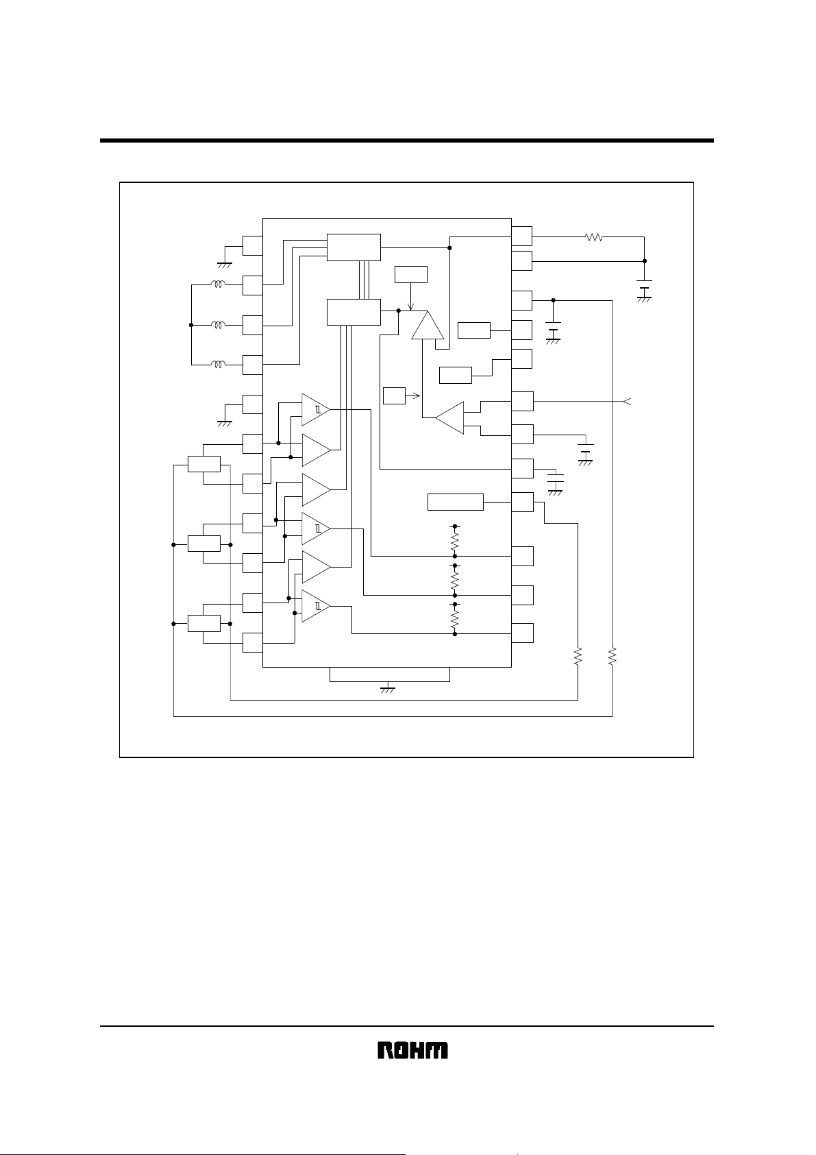
z
zBlock diagram
zz
BA6665FM
Hall 1
Hall 2
Hall 3
FIN
10
11
12
13
14
DRIVER
R
NF
27
28
3
GAIN
5
CONTROL
7
TSD
+
CURRENT
SENSE AMP
25
V
−
REV
24
CC
23
V
M
PS
8
9
+
−
+
−
TL
TORQUE
SENSE AMP
+
−
22
21
SERVO
SIGNAL
20
+
−
+
−
+
−
+
−
1.6kΩ
1.6kΩ
1.6kΩ
Hall Bias
VCC
(Typ.)
VCC
(Typ.)
VCC
(Typ.)
19
18
17
16
FIN
Page 3

Optical disc ICs
z
zPin descriptions
zz
BA6665FM
Pin No. Function
10
11
12
13
14
15
16
17
18
19
20
21
22
23
24
25
26
27
28
FIN
Pin Name
N.C.1
2
3
4
5
6
7
8
9
N.C.
A
N.C.
A
N.C.
A
GND
1
H
H
1
H
2
H
2
H
3
H
3
3
2
1
+
−
+
−
+
−
N.C.
FG3
FG2
FG1
H
V
C
NF
E
CR
E
C
PS
R
EV
V
CC
N.C.
V
M
R
NF
FIN
N.C.
N.C.
Output3 for motor
N.C.
Output2 for motor
N.C.
Output1 for motor
GND
Hall input Amp1. positive input
Hall input Amp1. negative input
Hall input Amp2. positive input
Hall input Amp2. negative input
Hall input Amp3. positive input
Hall input Amp3. negative input
N.C.
FG3 signal output terminal
FG2 signal output terminal
FG1 signal output terminal
Hall bias
Capacitor connection pin for phase compensation
Torque control standard voltage input terminal
Torque control voltage input terminal
START / STOP switch
Reverse terminal
Power supply for signal division
N.C.
Power supply for driver
Terminal connection for current sensing resistor
GND
Page 4

Optical disc ICs
z
zElectrical characteristics (unless otherwise noted, T a=25°C, VCC=5V , VM=12V)
zz
BA6665FM
Parameter Symbol Min.
TOTAL
Circuit current1
Circuit current2
POWER SAVE
ON voltage range
OFF voltage range
HALL BIAS
Hall bias voltage
HALL AMP
Input bias current
In−phase input voltage range
Minimum input level
H
hysteresis level
3
TORQUE CONTROL
Input voltage range
Offset voltage −
Offset voltage +
Input current
Input−output Gain
FG
FG output voltage H
FG output voltage L
OUTPUT
Saturation voltage H
Saturation voltage L
Pre−drive current
Torque limit current
REVERSE
ON voltage range
OFF voltage range
Max. Unit Conditions
Typ.
CC
1
E
E
E
V
V
V
V
C
COFF
COFF
V
V
V
V
I
CC
I
PSON
PSOFF
V
HB
I
HA
HAR
V
INH
HYS
, E
E
CIN
G
EC
FGH
FGL
V
OH
V
OL
I
VMP
I
TL
RSON
RSOFF
−
2
−
2.5
0.5
−
1.5
50
10
05
CR
−70 −40 −10
−
10 40
+ ECR=1.65V
−µA
0.56
4.5 4.9 5.0
0 0.25
−
−
−
560
2.5
−−
0.2
0
7.1
4.7
−
−
1.0
−−
0.9 1.5
0.7 3.0
4.0
−
−
−
20 40
−
70 mV
0.5
2.0
0.7 0.84
0.4
1.0 1.5
0.4
0.8
35
70
700 840
−−
1.0
mA
mA
V
V
V
µA
V
mVpp
mV
V
mV
A / V
V
V
V
V
mA
mA
V
V
At power save ON
At power save OFF
I
HB
=10mA
C
, ECR=0.5V~3.3V
E
E
CR
=1.65V
E
C=ECR
=1.65V
C
=1.3 , 1.5V 1.8 , 2.0V
E
RNF=0.5Ω
I
FG
=−20µA
FG
=3mA
I
I
O
=−600mA
O
=600mA
I
C
=5V output open
E
NF
=0.5Ω
R
Test Circuit
Fig.1
Fig.1
Fig.2
Fig.2
Fig.3
Fig.3
Fig.3
Fig.6
Fig.5
Fig.5
Fig.5
Fig.6
Fig.6
Fig.4
Fig.4
Fig.6
Fig.2
Page 5

Optical disc ICs
z
zMeasurement circuit
zz
5V
A1
12V
R
NF
A2
L
R
5V
1.65V
V2
I
HB
H1+ H2+ H3+
H1− H2− H3−
BA6665FM
ICC1 : Value of 'A1'
VPS=0 [V]
H1+~H3+=(1/2)×VCC+0.1 [V]
H1−~H3−=(1/2)×VCC [V]
ICC2 : Value of 'A1'
VPS=5 [V]
H1+~H3+=(1/2)×VCC+0.1 [V]
H1−~H3−=(1/2)×VCC [V]
VHB : Value of 'V2'
VPS=5 [V]
IHB=10 [mA]
V1
Circuit current
Fig.1
Hall bias voltage
5V
12V
NF
R
L
R
V
PS
V
REV
PS ON/OFF range
REV ON/OFF range
Fig.2
Torque limit current
E
C
Test Circuit
)
1.65V
H1+ H2+ H3+
Test Circuit
)
H1− H2− H3−
VPSON : Range of 'VPS' that output pins
become input-output table.
(Input condition 1~6)
VPSOFF : Range of 'VPS' that output pins
become open.
(Input condition 1~6)
VRSON : Range of 'VREV' that output pins
become input-output table.
(Input condition 1~6)
VPS=5 [V] EC=0 [V]
VRSOFF : Range of 'VREV' that output pins
become open.
(Input condition 1~6)
VPS=5 [V] EC=0 [V]
ITL : (Value of 'V1') / 0.5
VPS=5 [V] EC=0 [V]
(Input condition 1~6)
Page 6

Optical disc ICs
Input-output table
Input conditions
Pin No.
Condition 1
Condition 2
Condition 3
Condition 4
Condition 5
Condition 6
Cautions 1 : Regular EC<ECR REV = L, EC>ECR REV=H
Input voltage : Hi = 2.6V
9
10
11
12
13
H1+
H1−
H2+
H2−
H3+
L
M
H
M
M
H
M
L
M
M
M
M
L
M
H
M
M
H
M
L
H
M
M
M
L
L
M
M
M
H
Reverse EC<ECR REV = L,
Mid = 2.5V
Low = 2.4V
Regular Reverse
14
7
H3−
A1
A2
M
H
M
L
M
L
M
H
M
L
M
H
BA6665FM
Output
Test point
5
3
7
5
A3
A1
A2
L
L
L
H
H
H
H
L
H
L
H
L
L
H
L
H
L
H
H
H
H
L
L
L
3
A3
H
L
H
L
L
H
(Regular)
7pin HI
7pin Low
5pin HI
5pin Low
3pin HI
3pin Low
12V
5V
R
NF
L
R
Fig.3
1.65V
A
H1+ H2+ H3+
H1− H2− H3−
Input bias current
In-phase input voltage range
Hall minimum input level
A A A A A
Test Circuit
)
IHA : Value of 'A1' (Hn+=4.0V, Hn−=2.5V)
Value of 'A2' (Hn+=2.5V, Hn−=4.0V)
VHAR : Hall voltage range that output pins
become input-output table.
VINH : Hall input level that output pins
become input-output table.
Hn+−Hn− Hn−=2.5V (n=1, 2, 3)
n=1, 2, 3
Page 7

Optical disc ICs
5V
12V
R
NF
BA6665FM
1.65V
VOH : In case output measurement pin='H'
by input condition and IO=−600mA,
value of 'VOH'. (VM-RNF short)
VOL : In case output measurement pin='L'
by input condition and IO=600mA,
value of 'VOL'.
H1+ H2+ H3+
H1− H2− H3−
3, 5, 7pin
V
NF
R
12V
600mA
V
OH
M
V
Output saturation voltage H
Fig.4
Output saturation voltage L
5V
R
L
600mA
3, 5, 7pin
V
OL
GND
Test Circuit
)
E
C
1.65V
A
EC : Torque control operating. range.
H1+ H2+ H3+
H1− H2− H3−
ECOFF+, ECOFF− : Offset voltage at ECR=1.65V that
ECIN : Value of 'A' at EC=ECR=2.5V
GEC
: Value of 'V' at EC=1.3V→V1
Value of 'V' at EC=1.5V→V2
Value of 'V' at EC=1.8V→V3
Value of 'V' at EC=2.0V→V4
GEC={(V1−V2) / (1.5−1.3)} / RNF
GEC={(V4−V3) / (2.0−1.8)} / RNF
RNF=0.5Ω
value of 'V' become 3mV.
Torque offset voltage
Fig.5
Input-output gain
Test Circuit
)
Page 8

Optical disc ICs
A
12V
5V
R
NF
R
L
Hall hysteresis level
Pre-drive current
Fig.6
FG output voltage H
FG output voltage L
BA6665FM
VL
I
FG
E
C
1.65V
H1+ H2+ H3+
H1− H2− H3−
Test Circuit
)
VHYS : Difference Hn+ from Hn− that
FG1 / FG2 / FG3 voltage change. (n=1, 2, 3)
EC=ECR=1.65V
IVMp : value of 'A'
Output open
(Input condition 1~6)
EC=5V, ECR=2.5V
VFGL : Value of 'FG-OUTPUT-VOLTAGE'
at IFG=3mA (Hn+=L)
VFGH : Value of 'FG-OUTPUT-VOLTAGE'
at IFG=−20µA (Hn+=H)
zzzz
Electrical characteristic curves
7.5
(mA)
CC
5
2.5
CIRCUIT CURRENT : I
01234567
SUPPLY VOLTAGE : VCC (V)
Fig.7 Circuit Current
9
8
7
6
5
4
3
FG3 VOLTAGE : VFG3 (V)
2
1
−50 −40 −30−20 −10 0 10 20 30 40 50
H3 HYSTERESIS VOLTAGE ; H3+−H3− (mV)
Fig.10 H3 Hysteresis Level
5
9
8
(mA)
7
CC
6
5
4
3
2
CIRCUIT CURRENT : I
1
012345
PS VOLTAGE : VPS (V)
Fig.8 PS Threshold voltage
TL
(mA)
I
20
10
TORQUE LIMIT CURRENT (mA)
−50 0 +50
OFFSET VOLTAGE ; EC−ECR (mV)
Fig.11 Torque Control Offset voltage
EC−ECR (mV)
4
(V)
H
3
2
1
HALL BIAS VOLTAGE : V
0102030405060708090100
HALL BIAS CURRENT : IVH (mA)
Fig.9 Hall Bias voltage
900
TL
800
700
600
500
400
300
200
TORQUE LIMIT CURRENT : I
100
012345
TORQUE VOLTAGE : EC (V)
Fig.12 Torque Limit Current
Page 9

Optical disc ICs
(V)
OL
2.0
: V
OW
1.0
(V)
OH
1.0
OUTPUT CURRENT : IO (A)
1.0 2.0
(mA)
VM
100
BA6665FM
50
OUTPUT SATURATION VOLTAGE L
1.0 2.0
OUTPUT CURRENT : IO (A)
Fig.14 Output Saturation voltage Low
z
zExternal dimensions (Units : mm)
zz
18.5 ± 0.2
28 15
9.9 ± 0.3
7.5 ± 0.2
114
5.15 ± 0.1
0.35 ± 0.1
0.8
0.11
2.2 ± 0.1
HSOP-M28
0.3Min.
2.0
OUTPUT SATURATION VOLTAGE HIGH : V
Fig.13 Output Saturation voltage HI
0.25 ± 0.1
0.15
1.0 2.0
PRE-DRIVE CURRENT : I
10 20 30
VM SUPPLY VOLTAGE : VM (V)
Fig.15 Predrive Current
 Loading...