

Page 1
Motor driver ICs
FDD spindle motor driver
BA6477FS
The BA6477FS is a one-chip IC designed for driving FDD spindle motors. This high-performance IC employs a 3-phase,
full-wave soft switching drive system, and contains a digital servo, an index amplifier, and a power save circuit. The compactly packaged IC reduces the number of external components required.
Applications
Floppy disk drivers
Features
1) 3-phase, full-wave soft switching drive system.
2) Digital servo circuit.
3) Power save circuit.
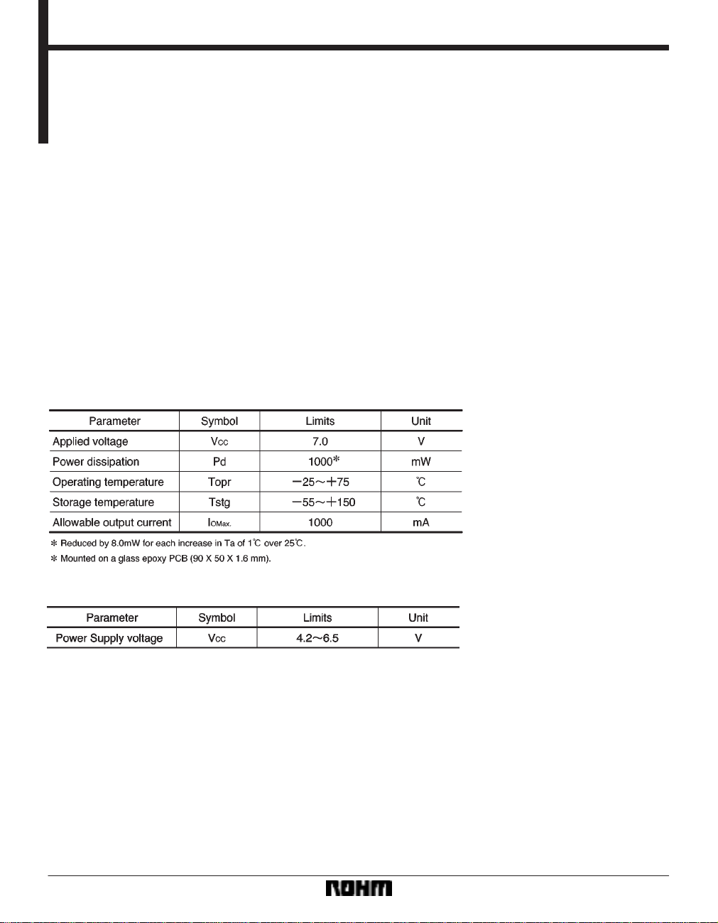
Absolute maximum ratings (Ta = 25C)
4) Hall power supply switch.
5) Motor speed changeable.
6) Index amplifier.
Recommended operating conditions (Ta = 25C)
532
Page 2
Motor driver ICs BA6477FS
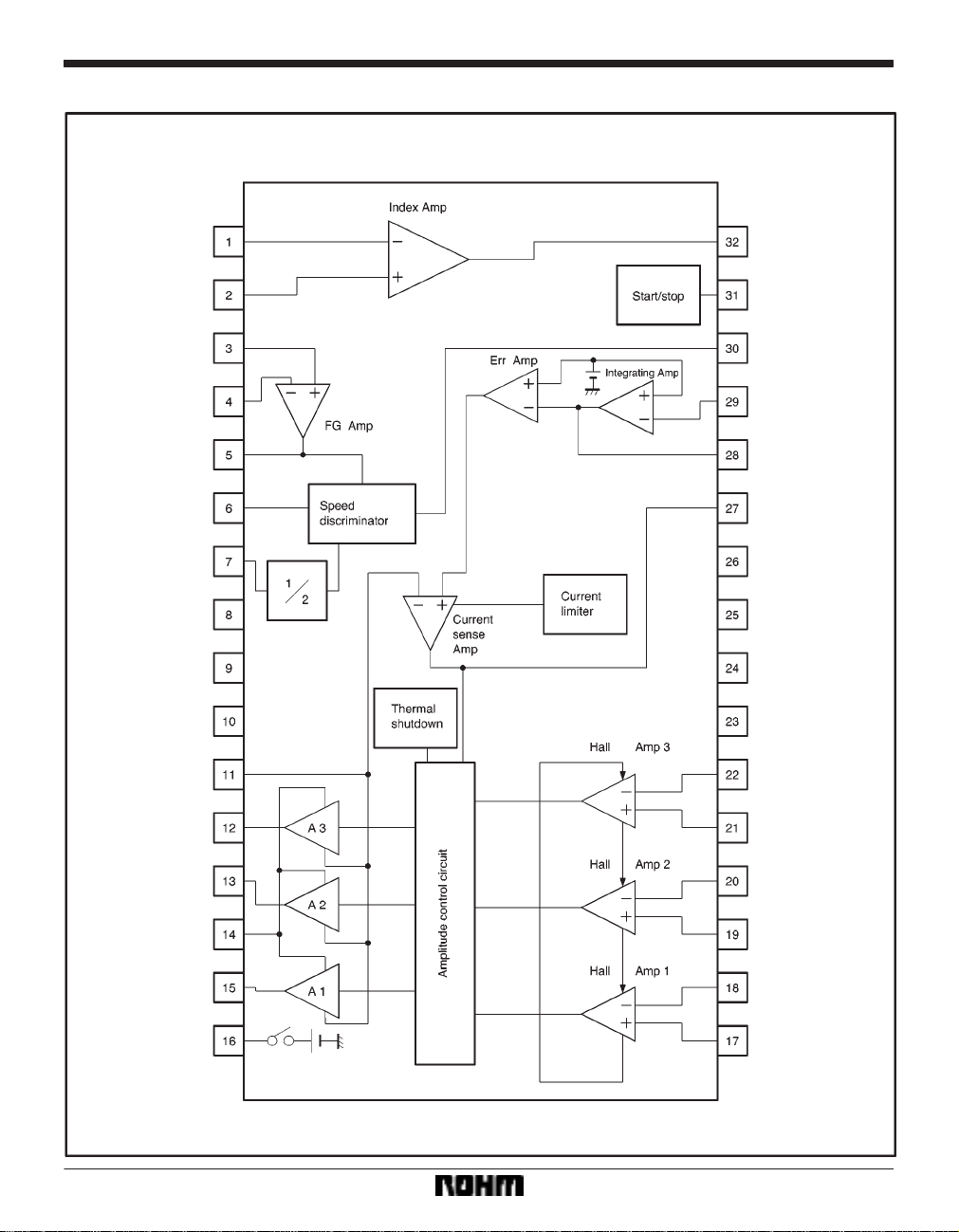
Block diagram
533
Page 3
Motor driver ICs BA6477FS
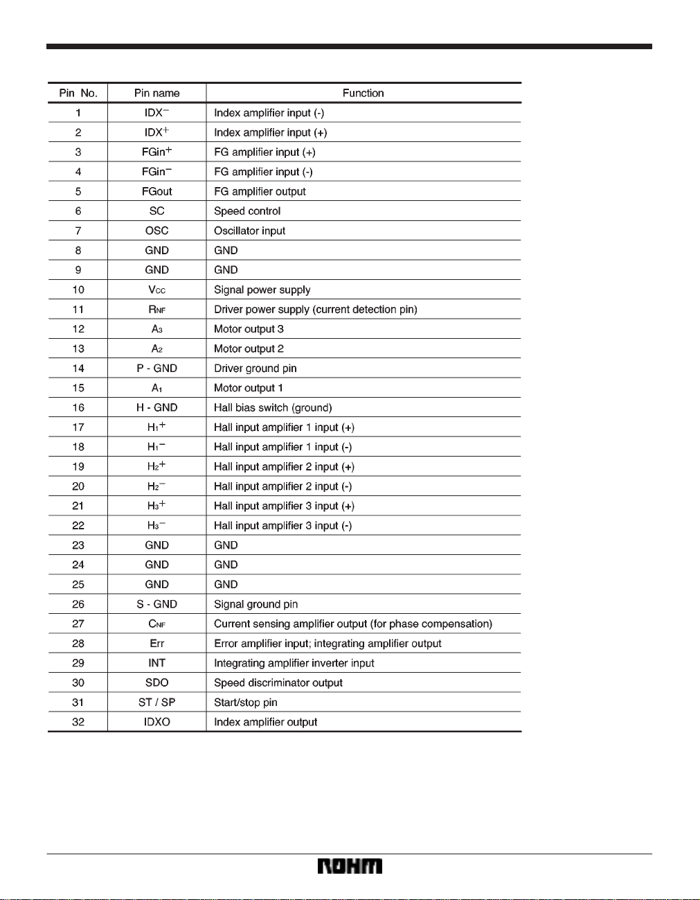
Pin descriptions
534
Page 4
Motor driver ICs BA6477FS
Input/output circuits
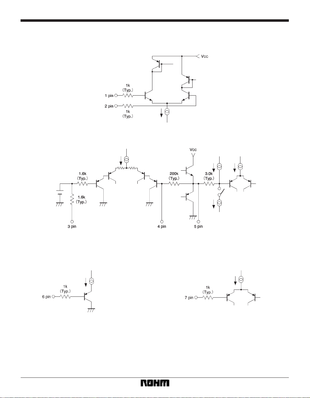
(1) Index input (1, 2 pin)
(2) FG amplifier (35 pin)
(3) Speed control (6 pin) (4) External clock input (7 pin)
535
Page 5

Motor driver ICs BA6477FS
(5) Motor output (1115 pin) (6) Hall bias (16 pin)
(7) Hall input (1722 pin) (8) Integrating amplifier (28, 29 pin)
(9) Speed discriminator output (30 pin) (10) Start/stop (31 pin) (11) Index output (32 pin)
536
Page 6

Motor driver ICs BA6477FS
Electrical characteristics (unless otherwise noted, Ta = 25C, VCC = 5V)
537
Page 7

Motor driver ICs BA6477FS
FCircuit operation
(1) Motor drive circuit
The motor driver is based on a 3-phase, full-wave soft
switching, current drive system in which the position of
rotor is sensed by Hall elements. The total drive current
of motor is sensed by a small resistor (R
NF) and regulated
through a voltage comparison. The IC consists of Hall
amplifiers, an amplitude control circuit, a driver, an error
amplifier, and a current feedback amplifier (Fig. 1).
The waveforms of different steps along the signal path
from the Hall elements to the motor driver output are
shown in Fig. 2. The Hall amplifiers receive the Hall elements voltage signals as differential signals. Next, by deducting the voltage signal of Hall elements 2 from the
voltage signal of Hall elements 1, current signal H1,
which has a phase 30 degrees ahead of Hall elements 1,
is created. Current signals H2 and H3 are created likewise. The amplitude control circuit then amplifies the H1,
H2, and H3 signal according to the current feedback amplifier signal. Then, drive current signals are produced at
A1, A2, and A3 by applying a constant magnification factor. Because a soft switching system is employed, the
drive current has low noise and a low total current ripple.
The total drive current is controlled by the error amplifier
input voltage. The error amplifier has a voltage gain of
about –1 1dB (a factor of 0.28). The current feedback amplifier regulates the total drive current, so that the error
amplifier output voltage (V1) is equal to the V
RNF voltage,
which has been voltage-converted from the total drive
current through the R
NF pin. If V1 exceeds the current lim-
iter voltage (Vcl), the constant voltage Vcl takes precedence, and a current limit is applied at the level of
NF.
Vcl / R
The current feedback amplifier tends to oscillate because it receives all the feedback with a gain of 0dB. To
prevent this oscillation, connect an external capacitor to
the C
NF pin for phase compensation and for reducing the
high frequency gain.
(2) Speed control circuit
The speed control circuit is a non-adjustable digital servo
system that uses a frequency locked loop (FLL). The circuit consists of an 1/2 frequency divider, an FG amplifier ,
and a speed discriminator (Fig. 3).
An internal reference is generated from an external clock
signal input. The 1/2 frequency divider reduces the frequency of the OSC signal. The FG amplifier amplifies the
minute voltage generated by the motor FG pattern and
produces a rectangular-shaped speed signal. The FG
amplifier gain (G
FG = 42dB, typical) is determined by the
internal resistance ratio.
For noise filtering, a high-pass filter is given by C3 and a
resistor of 1.6kΩ (typical), and a low-pass filter is given
by C4 and a resistor of 200kΩ (typical). The cutoff frequencies of high-pass and low-pass filters (f
H and fL, re-
spectively) are given by:
f
H =
2π 1.6kΩ
1
C3
fL =
2π 200kΩ C4
1
The C3 and C4 capacitances should be set so as to satisfy the following relationship:
HtfFGtfL
f
where fFG is the FG frequency . Note that the FG amplifier
inputs have a hysteresis.
The speed discriminator divides the reference clock and
compares with the reference frequency , and then outputs
an error pulse according to the frequency difference. The
motor rotational speed N is given in the following formula.
fosc
f
osc is the reference clock frequency,
n is (speed discriminator count)
1
(1)N = 60 S
S
n
z
2,
z is the FG tooth number.
The discriminator count depends on the speed control
pin voltage.
The integrator flattens out the error pulse of the speed
discriminator and creates a control signal for the motor
drive circuit (Fig. 4).
(3) Index amplifier
The index amplifier is a hysteresis amplifier with a typical
hysteresis width of +18mV and –22mV. The input pin is
not biased internally.
538
Page 8

Motor driver ICs BA6477FS
(4) Other circuits
S Start/stop circuit
The start /stop circuit puts the IC to the operating state
when the control pin is LOW, and to the standby state (circuit current is nearly zero) when the control pin is HIGH.
The Hall elements bias switch, which is linked to the
start/stop circuit, is turned off during the standby state,
so that the Hall device current is shut down.
FCircuit operation
S Thermal shutdown circuit
This circuit shuts down the IC currents when the chip
junction temperature is increased to about 175_C (typical). The thermal shutdown circuit is deactivated when
the temperature drops to about 155_C (typical).
539
Page 9

Motor driver ICs BA6477FS
540
Page 10

Motor driver ICs BA6477FS
Operation notes
(1) Thermal shutdown circuit
This circuit shuts down all the IC currents when the chip
junction temperature is increased to about 175C (typical). The thermal shutdown circuit is deactivated when
the temperature drops to about 155C (typical).
(2) Hall elements connection
Hall elements can be connected in either series or parallel. When connecting in series, care must be taken not to
allow the Hall output to exceed the Hall common-mode
input range.
(3) Hall input level
Switching noise may occur if the Hall input voltage (pins
1722) is too high. Differential inputs of about 100mV
P-P
are recommended.
(4) Driver ground pin (pin 14)
Pin 14, which is the motor current ground pin, is not connected to the signal ground pin (pin 26). Design a proper
conductor pattern in consideration of the motor current
that flows through pin 14.
(5) External clock
Make sure that the pin7 voltage is always less than V
and more than the ground voltage.
CC
541
Page 11

Motor driver ICs BA6477FS
Application example
542
Page 12

Motor driver ICs BA6477FS
Electrical characteristic curves
External dimensions (Units: mm)
543
 Loading...