

Page 1
Motor driver ICs
3-phase motor driver
BA6458FP-Y
The BA6458FP-Y is an one-chip IC designed for driving video cassette recorder cylinder motors. It is a high-performance
IC with a 3-phase, full-wave, pseudo-linear drive system. The IC is compactly packaged.
Applications
Video cassette recorder cylinder motors
Features
1) 3-phase, full-wave, pseudo-linear drive system.
2) Output saturation voltage is low with low variation.
3) Built-in torque limit pin.
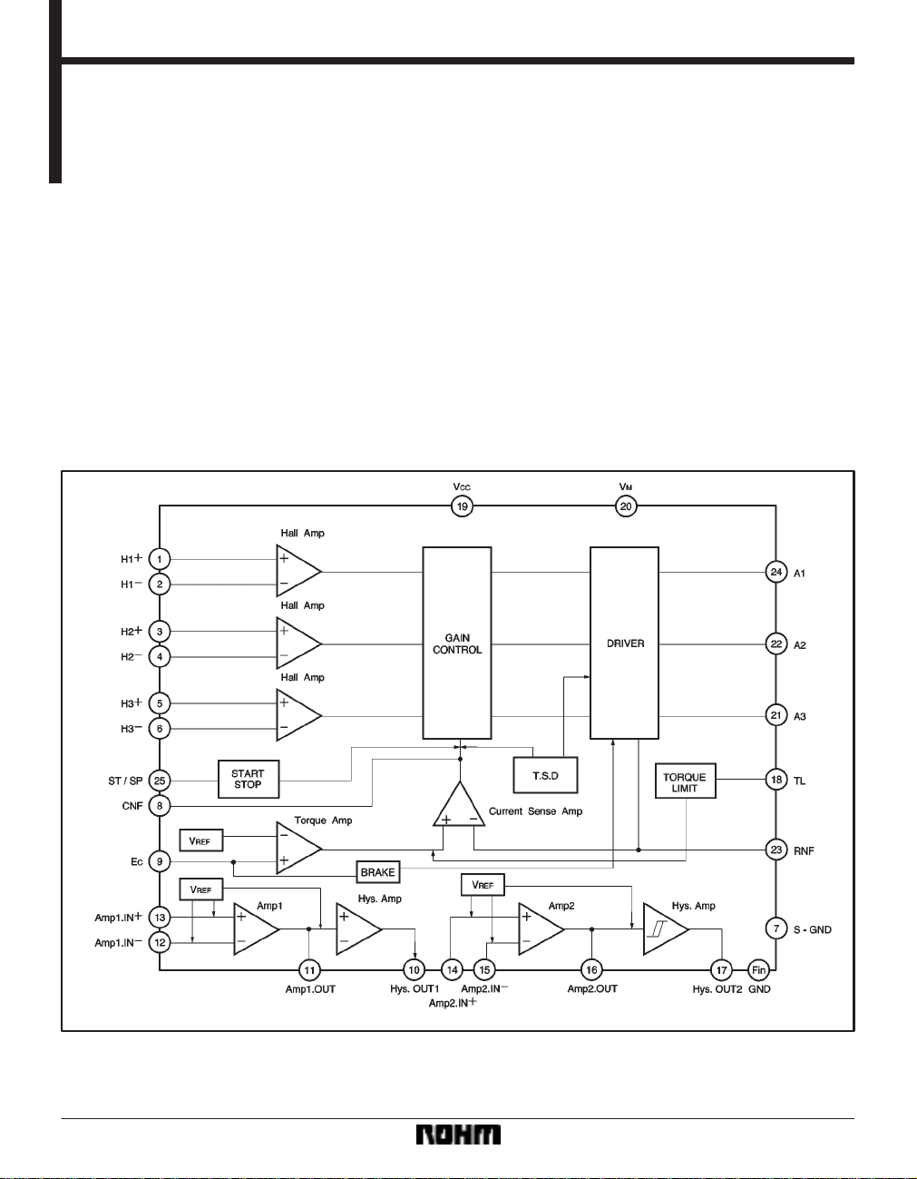
Block diagram
4) Contains two amplifiers and two hysteresis amplifiers to amplify FG and PG signals.
5) Built-in thermal shutdown circuit.
603
Page 2
Motor driver ICs BA6458FP-Y
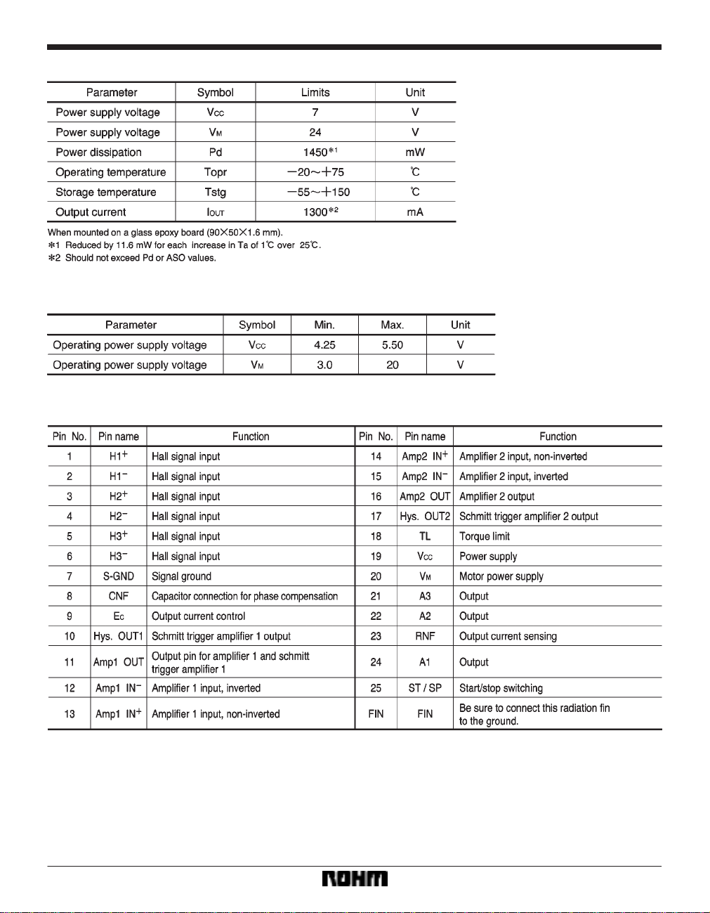
FAbsolute maximum ratings (Ta=25_C)
FRecommended operating conditions (Ta=25_C)
FPin descriptions
604
Page 3

Motor driver ICs BA6458FP-Y
FElectrical characteristics (unless otherwise noted, Ta=25_C, VCC=5V, VM=12V)
605
Page 4

Motor driver ICs BA6458FP-Y
Circuit operation
(1) The 3-phase Hall signal is amplified in the hall amplifiers and sent to the matrix section, where the signal is
further amplified and combined. After the signal is converted to a current in the amplitude control circuit, the current is supplied to the output driver, which then provides
a motor drive current. The phases of the Hall input signal,
output voltage, and output current are shown in Fig. 1.
(2) Torque control pin
The output current can be controlled by adjusting the
voltage applied to the torque control pin (pin 9).
(3) Start/stop pin
The motor is in the run mode when the pin input voltage
is 3.5V or more and in the idle mode (all output transistors
are off) when the voltage is 1.2V or less.
(4) Power ground pin (R
NF pin is the output stage ground pin. Connect a re-
The R
NF pin)
sistor (0.5Ω recommended) between this pin and the
ground to monitor the output current.
(5) Torque limit pin (TL pin)
The output current can be limited by applying a voltage
to the torque limit pin. Control is provided so that this pin
will have the same potential as the R
NF pin. Note that
there is an offset in the TL-pin voltage.
(6) Phase compensation pin (C
Connect a capacitor between this pin and V
NF pin)
CC if the out-
put tends to oscillate.
(7) Amplifiers 1 and 2
Amplifiers 1 and 2 have an open loop gain of about 70dB
(typical). The input terminals are biased internally to
2.45V (typical).
(8) Hysteresis amplifiers
The hysteresis amplifiers have a hysteresis width of
±120mV (typical). The input terminals are biased internally.
606
Page 5

Motor driver ICs BA6458FP-Y
Operation notes
(1) Input/output circuit
(1) Start/stop switching pin (25 pin)
(4) Driver output (A1: 24 pin, A2: 22 pin, A3: 21 pin)
(2) Torque limit pin (18 pin)
(3) Torque control input (9 pin)
(5) Hall input
+
(H1
: 1 pin, H1: 2 pin, H2+: 3 pin, H2: 4 pin,
+
: 5 pin, H3: 6 pin)
H3
(6) I/O of amplifiers 1 and 2
607
Page 6

Motor driver ICs BA6458FP-Y
(7) I/O of hysteresis amplifiers
(5) Torque limit pin (pin 18)
∗ Note that resistance values of the I/O circuits can vary
± 30%
(2) Torque control
The R
NF-pin output voltage is plotted against the torque
control input voltage (E
C) in Fig. 10.
The output current can be limited by applying a voltage
to the torque limit pin. Control is provided so that this pin
will have the same potential as the power ground pin.
Note that there is a voltage offset on this pin. The R
NF-pin
voltage is 0.325V when the TL-pin voltage is 0.4V (typi-
cal) and the R
age offset changes with the R
NF-pin resistance is 0.5Ω. Note that the volt-
NF-pin resistance.
(3) Start/stop pin
The I/O equivalent circuit of the start/stop pin is shown
in (1). 1) of “Precautions for use.” The pin has a temperature dependence of *7mV/_C, and the resistance can
vary ±30%. Take the temperature effect into consideration when designing your application.
(4) Hall input
The I/O equivalent circuit of the Hall input pins is shown
in (1). 5) of “Precautions for use.” The Hall devices can
be connected in either series or parallel.
(6) Amplifiers 1 and 2
Unpredictable outputs may occur when the amplifier in-
put is outside the recommended range.
(7) Hysteresis amplifier
An input range of 0.6V to (V
CC X 1.2V) is recommended.
Unpredictable outputs may occur when the input is out-
side this range.
(8) Thermal shutdown circuit (TSD)
The circuit puts the driver outputs (A1, A2, and A3) to the
open state at the temperature of 175_C (typical). There
is a temperature difference of about 20_C between the
temperatures at which the circuit is activated and deacti-
vated.
608
Page 7

Motor driver ICs BA6458FP-Y
Application example
609
Page 8

Motor driver ICs BA6458FP-Y
Electrical characteristic curves
External dimensions (Units: mm)
610
 Loading...