

Page 1
1
Standard ICs
6-channel inverter
BA6266 / BA6266F
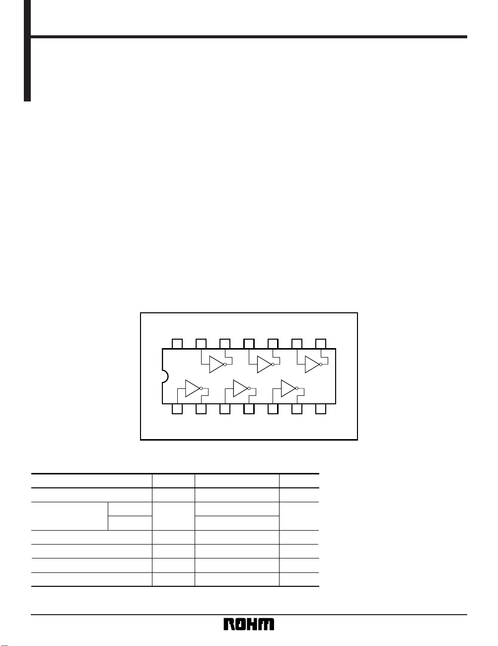
The BA6266 and BA6266F are driver ICs featuring high output voltage capability and high-current open collector output, and having six built-in inverter buffer circuits.
The open collector output enables “AND” ties. In addition, clamp diodes are connected to all inputs, minimizing error
caused by ringing and other factors. These inverters feature a high output pressure withstand resistance of 30V, as
well as a large output power supply (sink current) of 40mA, making them suitable for use in LED drivers and interfaces with other elements.
•
Applications
General-purpose digital equipment
•
Features
1) High output current. (I
OL = 40mA)
2) High output voltage. (V
O = 30V)
3) “AND” ties enabled.
4) Wide range of operating temperatures.
•
Block diagram
1414 13 12 11 10 9 8
76543211
6A 6Y 5A 5Y 4A 4Y
1A 1Y 2A 2Y 3A 3Y GND
∗
∗
∗
∗
∗
∗
V
CC
∗ Open collector
•
Absolute maximum ratings (Ta = 25°C)
Parameter Symbol Limits Unit
Power supply voltage V
CC 7V
BA6266 600
∗
1
BA6266F 550
∗
2
Input voltage VI 5.5 V
Output voltage V
O 33 V
Operating temperature Topr 0 ~ + 70 °C
Storage temperature Tstg
– 55 ~ + 125
°C
Power dissipation Pd mW
∗
1 Reduced by 6.0mW for each increase in Ta of 1°C over 25°C.
∗
2 Reduced by 5.5mW for each increase in Ta of 1°C over 25°C.
Page 2
2
Standard ICs BA6266 / BA6266F
•
Recommended operating conditions (Ta = 25°C, VCC = 5V)
Parameter Symbol Min. Typ. Max. Unit Conditions
Power supply voltage V
CC 4.75 5 5.25 V —
Output voltage V
O ——30 V When output is "H"
•
Electrical characteristics (unless otherwise noted, Ta = 25°C, VCC = 5V)
Parameter Symbol Min. Typ. Max. Unit Conditions
Input high level voltage V
IH 2 ——V
Input low level voltage V
IL ——0.8 V
—
—
Output saturation voltage 1 V
OL1 ——0.4 V VCC = 4.75V, IOL = 16mA
Output saturation voltage 2 VOL2 ——0.7 V VCC = 4.75V, IOL = 40mA
•
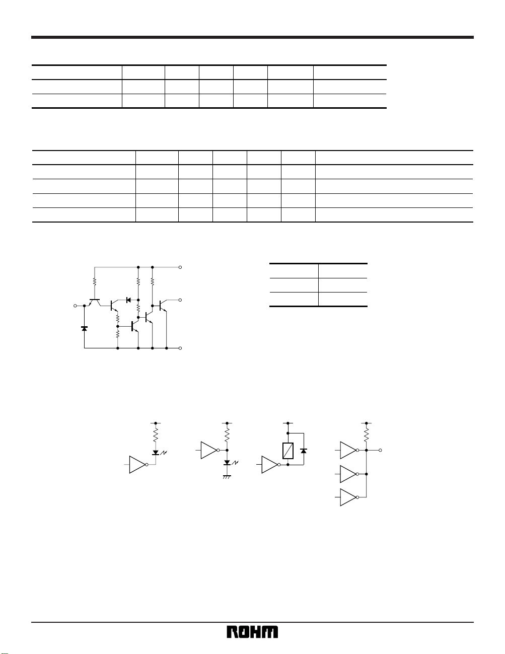
Internal equivalent circuit diagram
100Ω
1kΩ
1.6kΩ
2kΩ
1.4kΩ
9kΩ
GND
Y Output
Input A
V
CC
(Resistance values are typical values.)
Fig.1
•
Truth table
AY
HL
LH
•
Application examples
LED driver 1 LED driver 2 Relay driver
AND tie
Fig.2
Page 3

3
Standard ICs BA6266 / BA6266F
•
Electrical characteristics curves
–25 0 25 50 75 100 125
100
200
300
400
500
600
BA6266
BA6266F
POWER DISSIPATION : Pd (mW)
AMBIENT TEMPERATURE : Ta (°C)
Fig.3 Power dissipation vs.
ambient temperature
10020 40 60 80
50
40
30
20
10
0
BA6266
BA6266F
When all outputs are on
Ta = 70°C
OUTPUT CURRENT : IOL (mA)
DUTY CYCLE (%)
Fig.4 Output conditions diagram
•
External dimensions (Units: mm)
BA6266 BA6266F
DIP14 SOP14
6.5 ± 0.3
19.4 ± 0.3
0.5 ± 0.1
3.2 ± 0.2
4.25 ± 0.3
14 8
71
0.3 ± 0.1
0.51Min.
7.62
0° ~ 15°
2.54
0.4
± 0.11.27
1
14
8.7 ± 0.2
7
8
4.4 ± 0.2
6.2 ± 0.3
0.11
1.5 ± 0.1
0.15
0.15 ± 0.1
0.3Min.
 Loading...