

Page 1
Audio ICs
2-channel head switch for radio
cassette recorders
BA3126F / BA3126N
The BA3126F and BA3126N are dual-channel tape head switching ICs designed for use in radio cassette players.
These ICs are designed to withstand voltages of up to 120V
recording. Both devices have two channels, and are ideal for use in radio-cassette players.
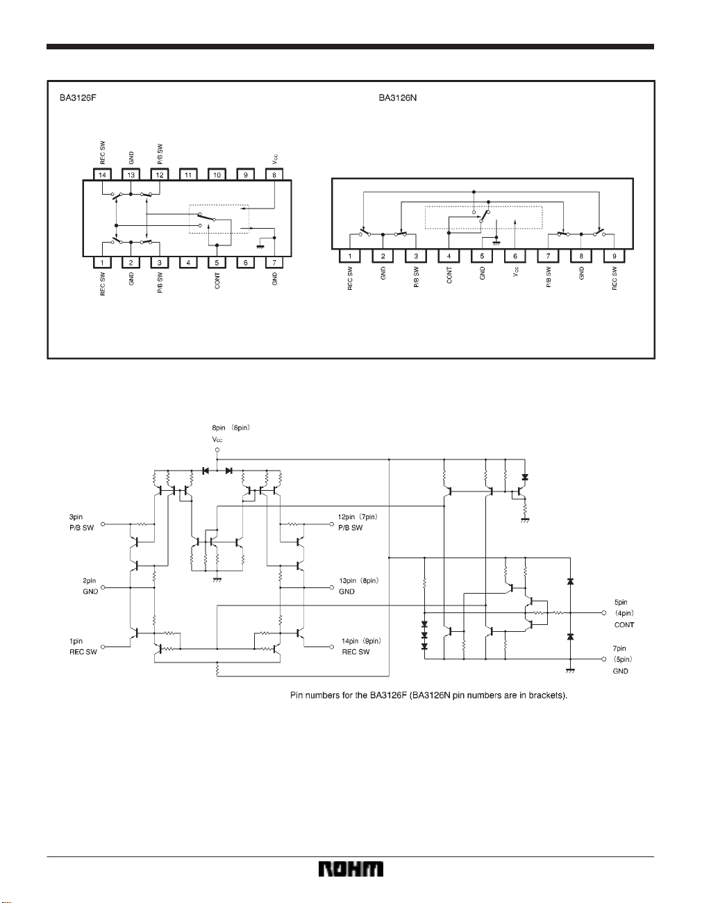
The package types are 14-pin SOP for the BA3126F, and 9-pin SIP for the BA3126N.
Applications
Radio-cassette players
Features
1) High withstanding voltage
P-PMin. at f = 100kHz).
(120V
2) Low “on” resistance (P / B SW : 8Ω,
REC SW : 5Ω)
P-PMin., and can handle large-amplitude bias signals during
3) Low offset voltage (P/B SW : 5.0mV,
REC SW : 0.6mV)
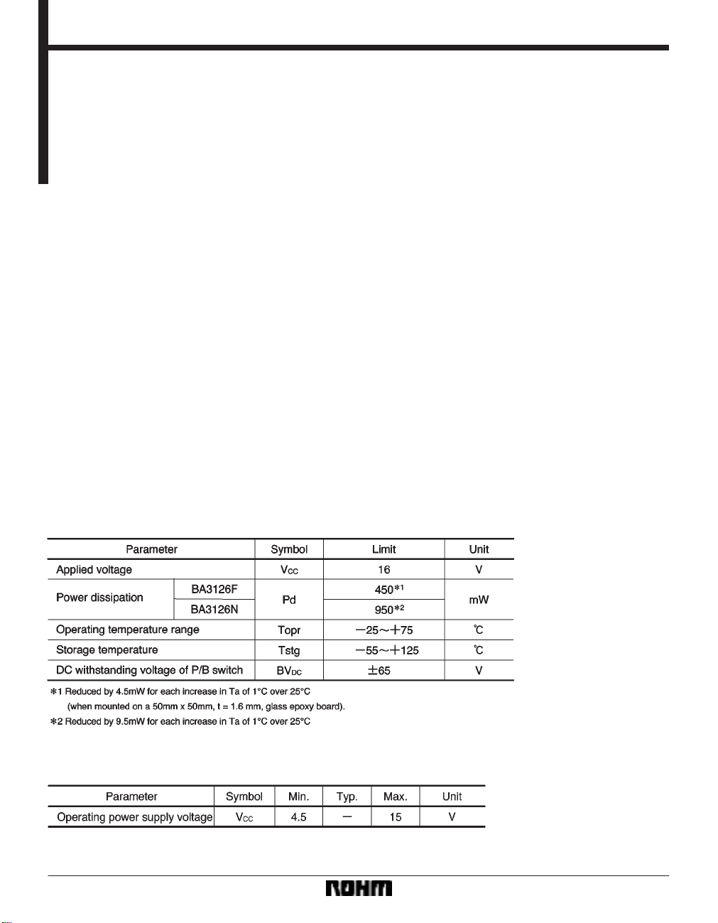
Absolute maximum ratings (Ta = 25C)
Recommended operating conditions (Ta = 25C)
818
Page 2
Audio ICs BA3126F / BA3126N
Block diagram
Internal circuit configuration
819
Page 3
Audio ICs BA3126F / BA3126N
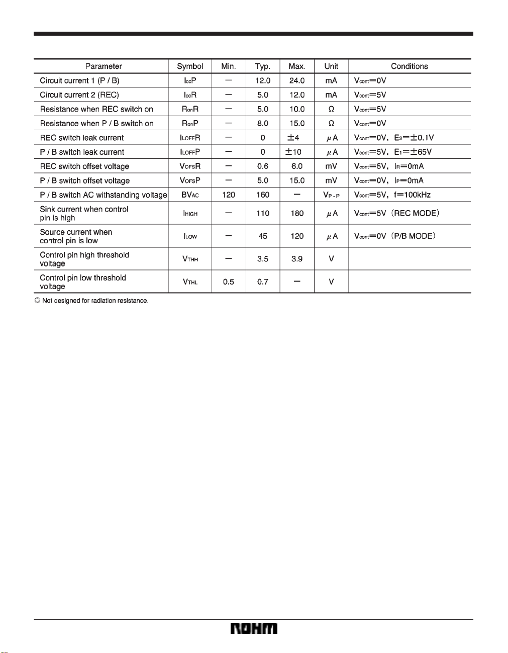
Electrical characteristics (unless otherwise noted, Ta = 25C, VCC = 9.0V, measurement circuit : Figs. 7 and 8).
820
Page 4

Audio ICs BA3126F / BA3126N
Measurement circuit
821
Page 5

Audio ICs BA3126F / BA3126N
Circuit operation
(1) Playback mode
When the control pin voltage goes below 0.5V , the REC
SW goes off and the P / B SW goes on to put the IC into
playback mode. In this mode, the playback signal from
the head is sent to the P / B amplifier via the REC SW.
Operation notes
(1) When the voltage on the control pin drops below
0.5V , (pin 5 for the BA3126F , and pin 4 for the BA3126N)
the IC switches to P / B mode . When the voltage is 0V,
the maximum source current generated is 120µA (I
LOW).
When the voltage on the control pin goes above 3.9V the
IC switches to REC mode. When the voltage is 5V, the
maximum sink current generated is 180µA (I
the control pin is open, the voltage on it is 3V
HIGH). When
F (approxi-
mately 2.0V). All switches are on at this time.
(2) P / B switch (BA3126F : pins 3 and 12, BA3126N
: pins 3 and 7)
This switch is on during playback. Due to the characteristics of the transistor switch, the following DC voltage is
generated :
V
OFSP < 15mV (VCC = 9.0V, Vcont = 0V)
This switch is off during recording. A built-in, high-withstanding voltage switch means that it can handle the
large-amplitude bias signal generated by the bias generator.
Due to variations between individual ICs, we recommend
that you keep the voltage below 120V
P-P (at f = 100kHz).
(3) REC switch (BA3126F : pins 1 and 14, BA3126N :
pins 1 and 9)
This switch is on during recording. Due to the characteristics of the transistor switch, the following DC voltage is
generated :
V
OFSP < 6mV (VCC = 9.0V, Vcont = 5V)
The switch is off during playback, and the playback signal
from the head is transmitted to the playback amplifier.
(2) REC mode
When the control pin voltage goes above 3.9V , the P / B
SW goes off and the REC SW goes on to put the IC into
record mode. In this mode, the recording signal from
REC amplifier is transmitted to the head via the P / B
SW.
(4) Recommended operating power supply voltage
range
Operation of the basic functions of the application example circuit are guaranteed if operated within the stipulated
power supply voltage and ambient temperature ranges.
We cannot guarantee the ratings for the electrical characteristics, but they will not change radically if the circuit
is operated within the stipulated power supply voltage
and ambient temperature ranges.
(5) Transient characteristics during power supply
switching
When the power is switched on and of in P / B mode
(control pin low), a transient current may flow from the
P / B SW to the REC SW.
If the head is in contact with the tape, and this current
flows into the head, the frequency component will be recorded as a pop sound on the tape. Pay due consideration to the power supply on / off timing and the head
position relationship.
(6) Playback-to-recording switching timing
If a large-amplitude signal from the bias oscillator is applied when the P / B SW is on, the P / B switch may latch
if there is excessive current from the bias oscillator. If this
happens, the P / B SW will not switch off when the control pin is driven high, and the IC will not enter REC mode.
Design the timing so that when the IC is switched from
playback to recording mode, the P / B SW goes off before the large-amplitude signal from the bias oscillator is
applied to the P / B SW.
822
Page 6

Audio ICs BA3126F / BA3126N
Application example
823
Page 7

Audio ICs BA3126F / BA3126N
Electrical characteristics curves
External dimensions (Units: mm)
824
 Loading...