

Datasheet B8390K6-5.9, B8390K6-5.8, B8390K6-5.7, B8390K6-5.6, B8390K6-5.5 Datasheet (BAYLI)
...Page 1
Bay Linear, Inc
2418 Armstrong Street, Livermore, CA 94550 Tel: (925) 606-5950, Fax: (925) 940-9556 www.baylinear.com
Surface Mount RF PIN Switch Diodes
B8390
Series
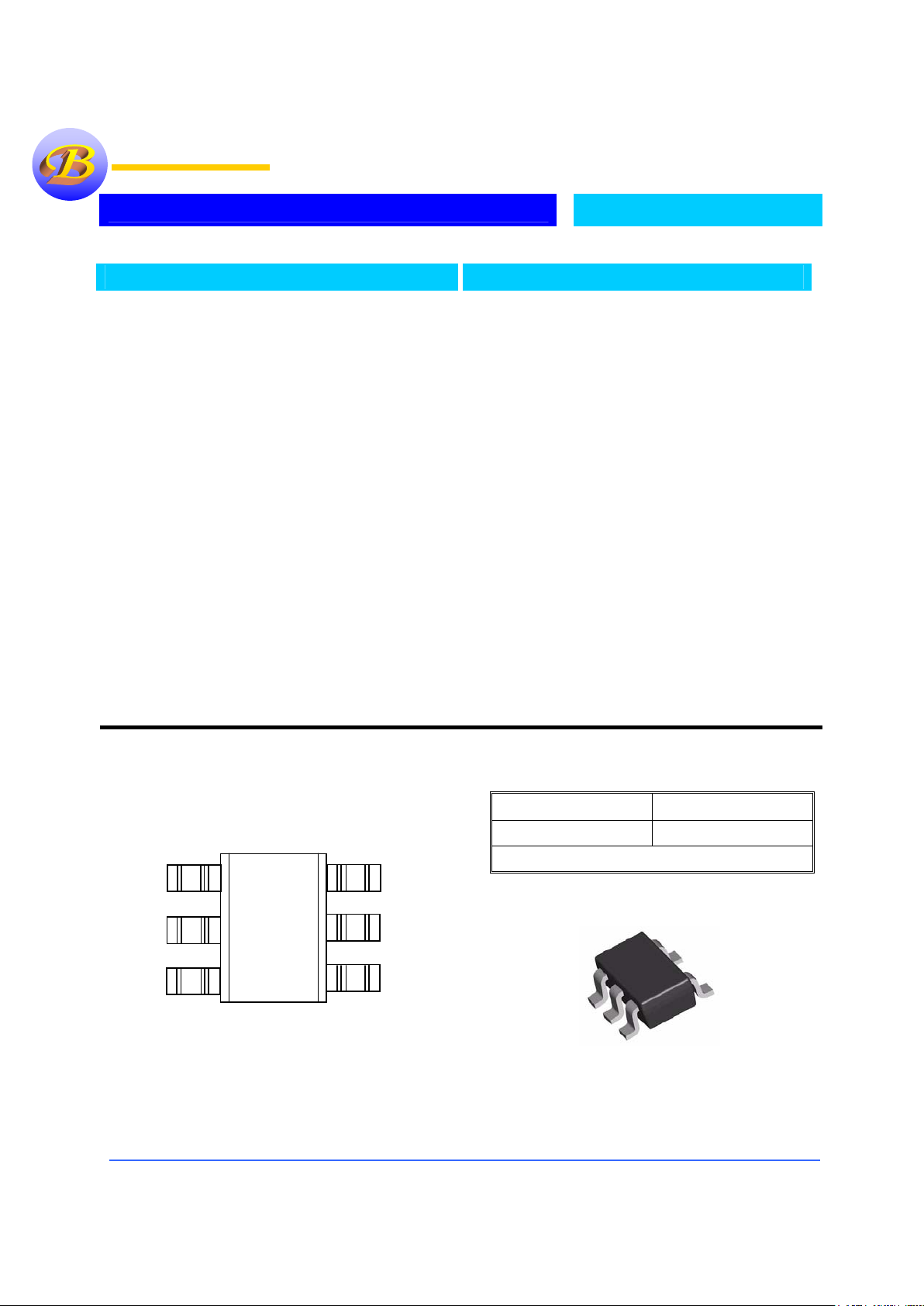
Pin Connection
Ordering Information
Package Part No.
SOT-26 B839XK6 -X.X
Description
The B-839x series is optimized for switching
applications where low resistance at low current and low
capacitance are required. The B-849x series products
feature ultra low parasitic inductance. These products
are specifically designed for use at frequencies which
are much higher than the upper limit for conventional
PIN diodes.
At Bay Linear, our commitment to quality components
gives our customers a reliable source of RF products,
which are tested at a more stringent level than our
competitors. Manufacturing techniques assure that when
two diodes are mounted into a single package they are
taken from adjacent sites on the wafer.
In cross referenced parts, we guarantee pin to pin
compatibility. The various package configurations
available provide a low cost solution to a wide variety of
design problems.
Features
• Unique Configurations in Surface Mount
• Add Flexibility
• Save Board Space
• Reduce Cost
• Switching
• Low Capacitance
• Low Resistance at Low Current
• Low Failure in Time (FIT) Rate
• Matched Diodes
• High Thermal Conductivity for greater Power
Bay Linear
Inspire the Linear Power
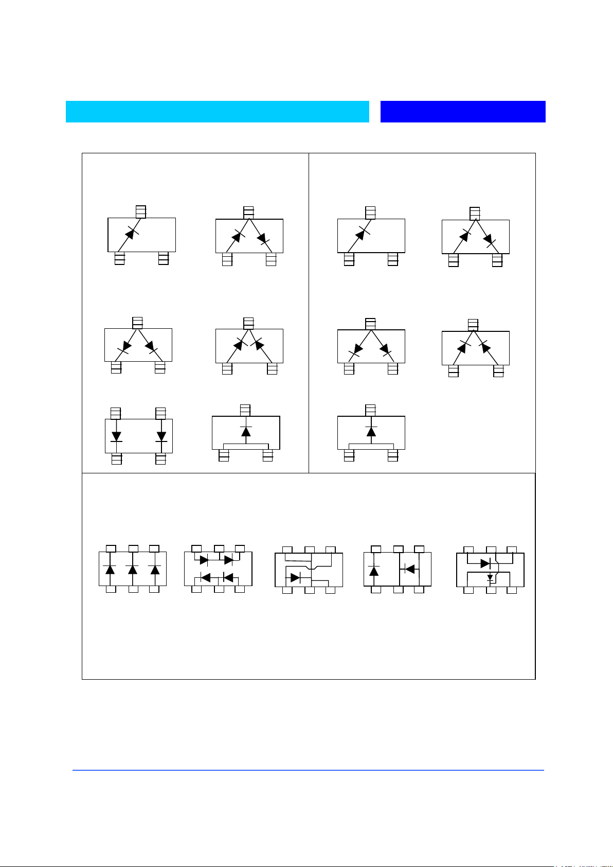
Pin Connections and
Package Marking
Notes:
1. Package marking provides
orientation and identification
2. See “Electrical Specifications”
for appropriate package marking
3
1
2
4
5
6
C4Z
3
1
2
4
5
6
C4ZC4Z
Page 2
Bay Linear, Inc
2418 Armstrong Street, Livermore, CA 94550 Tel: (925) 606-5950, Fax: (925) 940-9556 www.baylinear.com
B8390
SERIES
SOT-323 Package Lead
Code Identification (top view)
SINGLE
3
12
SOT-363 Package 6 Lead
Code Identification (top view)
UNCONNECTED
TRIO
BRIDGE
QUAD
1
3
56
2
4
1
3
56
2
4
SOT-23/SOT-143 Package
Lead Code Identification (top view)
3
12
COMMON
ANODE
COMMON
CATHODE
DUAL ANODE
3
12
12
3
12
3
UNCONNECTED
PAIR
3
12
3
12
COMMON
ANODE
COMMON
CATHODE
3
12
DUAL ANODE
12
3
12
3
3
12
SINGLE
3
12
SERIES
132
LOW
INDUCTANCE
SINGLE
654
1
3
56
2
4
SERIES-
SHUNT PAIR
132
654
HIGH
FREQUENCY
SERIES
Page 3

Bay Linear, Inc
2418 Armstrong Street, Livermore, CA 94550 Tel: (925) 606-5950, Fax: (925) 940-9556 www.baylinear.com
B8390
Absolute Maximum Ratings
Parameter Symbol SOT-23/143 SOT-323 Units
Peak Inverse Voltage P
IV
100 100 V
Junction Temperature T
J
150 150 °C
Storage Temperature T
STG
-65 to 150 -65 to 150 °C
Forward Current (1us puls) I
F
1 1 Amp
Thermal Resistance[2] θjc 500 150 °C/W
DC Electrical Specifications (TC = 25°C, Single Diode)
Part No.
Package
Marking
Configuration
Maximum
Forward Voltage
VF (mV)
Typical Capacitance
CT (pF)
8390
8392
8393
8394
8395
8391
8396
8397
8398
839A
839B
839C
839D
839E
Single
Series
Common Anode
Common Cathode
Unconnected Pair
Single
Series
Common Anode
Common Cathode
Unconnected Trio
Dual Switch Mode
Low Inductance Single
Series Shunt Pair
High Frequency Series
100 2.5
0.30
Test Conditions
VR= VBR IF= 5mA
f =100 MHz
Measure
IR< 10µA
V
F
=5Volt
F=1 MHz
Typical Parameter, TC = +25°C,
Part Number
Series Resistance
R
S
Carrier Lifetime
t (ns)
Total Capacitance
CT (pF)
839X 3.8 200 0.2 @5Volt
Test Conditions
I
F
= 1.0 mA
f = 100 MHz
IF = 10 mA
I
R
= 6 mA
High Frequency (Low Inductance, 500 MHz – 3GHz) PIN Diodes
Part No. Config. Min.
B.Voltage
VBR (V)
Max. Series
Resistance
Rs
Typical
Capacitance
CT (pF)
Max.
Capacitance
CT (pF)
Typical
Inductance
LT (pF)
849X Dual Anode 100 2.5 0.33 0.375 1.0
Test Conditions
V
R
= VBR
I
R
< 10µA
I
F
= 5mA
VR= 5V
f =1 MHz
VR= 5V
f =1 MHz
f =500 MHz
3GHz
Page 4

Bay Linear, Inc
2418 Armstrong Street, Livermore, CA 94550 Tel: (925) 606-5950, Fax: (925) 940-9556 www.baylinear.com
B8390
Graph 1: Typical Forward Current
vs. Forward Voltage
VF - Forward Voltage (V)
I
F
– Forward Current (mA)
100
10
1
0.1
0.01
00.2 0.80.60.4 1.0 1.2
125 C 25 C -50 C
Graph 1: Typical Forward Current
vs. Forward Voltage
VF - Forward Voltage (V)
I
F
– Forward Current (mA)
100
10
1
0.1
0.01
00.2 0.80.60.4 1.0 1.2
125 C 25 C -50 C
Graph 3: Total RF Resistance at 25 C vs.
Forward Bias Current.
IF– Forward Bias Current (mA)
100
10
1
0.1
0.01
0.1
10
RF Resistance (Ohms)
1001
Graph 4: Capacitance vs.
Reverse Voltage
VR– Reverse Voltage (V)
04
81216
20
0.20
0.25
0.30
0.35
0.40
0.45
0.50
0.55
Total Capacitance (pF)
1 MHz
1 GHz
Page 5

Bay Linear, Inc
2418 Armstrong Street, Livermore, CA 94550 Tel: (925) 606-5950, Fax: (925) 940-9556 www.baylinear.com
B8390
Cross Reference
Bay Part Number Agilent Part Number
B8390 HSMP3890
B8391 HSMP 389B
B8392 HSMP 3892
B8393 HSMP 3893
B8394 HSMP 3894
B8395 HSMP 3895
B8396 HSMP 389C
B8397 HSMP 389E
B8398 HSMP 389F
B839A HSMP 389L
B839B HSMP 389R
B839C HSMP 389T
B839D HSMP 389U
B839E HSMP 389V
B8490 HSMP 4890
B849A HSMP 489B
RT=0.5 + R
J
CT= CP+C
J
RJ= 20 / I
0.9
Ohms
where
I = Forward Bias Current in mA
Ib+ I
s
R
j
C
j
R
S
0.12 pF
0.5 Ohms
Page 6

Bay Linear, Inc
2418 Armstrong Street, Livermore, CA 94550 Tel: (925) 606-5950, Fax: (925) 940-9556 www.baylinear.com
Advance Information- These data sheets contain descriptions of products that are in development. The specifications are based on the engineering calculations,
computer simulations and/ or initial prototype evaluation.
Preliminary Information- These data sheets contain minimum and maximum specifications that are based on the initial device characterizations. These limits are
subject to change upon the completion of the full characterization over the specified temperature and supply voltage ranges.
The application circuit examples are only to explain the representative applications of the devices and are not intended to guarantee any circuit
design or permit any industrial property right to other rights to execute. Bay Linear takes no responsibility for any problems related to any
industrial property right resulting from the use of the contents shown in the data book. Typical parameters can and do vary in different
applications. Customer’s technical experts must validate all operating parameters including “ Typical” for each customer application.
LIFE SUPPORT AND NUCLEAR POLICY
Bay Linear products are not authorized for and should not be used within life support systems which are intended for surgical
implants into the body to support or sustain life, in aircraft, space equipment, submarine, or nuclear facility applications without
the specific written consent of Bay Linear President.
 Loading...