

Page 1
■ HIGH SPEED:t
at V
■ ON RESISTANCE BETWEEN TWO PORT:
=4.5VTA=85°C
CC
5Ω (TYP)at V
■ LOW POWER DISSIPATION:
I
= 1uA(MAX.) at TA=25°C
CC
■ COMPATIBLE WITH TTL OUTPUTS:
V
=2V(MIN), VIL=0.8V(MAX)
IH
■ POWER DOWN PROTECTION ON INPUTS
= 0.25ns (MAX.)
PD
=5.0VTA=25°C
CC
AND OUTPUTS
■ OPERATING VOLTAGE RANGE:
V
(OPR) = 4V to 5.5V
CC
■ PIN AND FUNCTION COMPATIBLE WITH
74 SERIES 16861
■ IMPROVED LATC H-UP IMMUNITY
■ ESD PERFORMANCE:
HBM > 2000V (MIL STD 883 method 3015);
MM > 200V
B5S16861
20-BIT TWO PORT BUS SWITCH
PRELIMINARY DATA
TSSOP
ORDER CODES
PACKAGE T & R
TSSOP48 B5S16861TTR
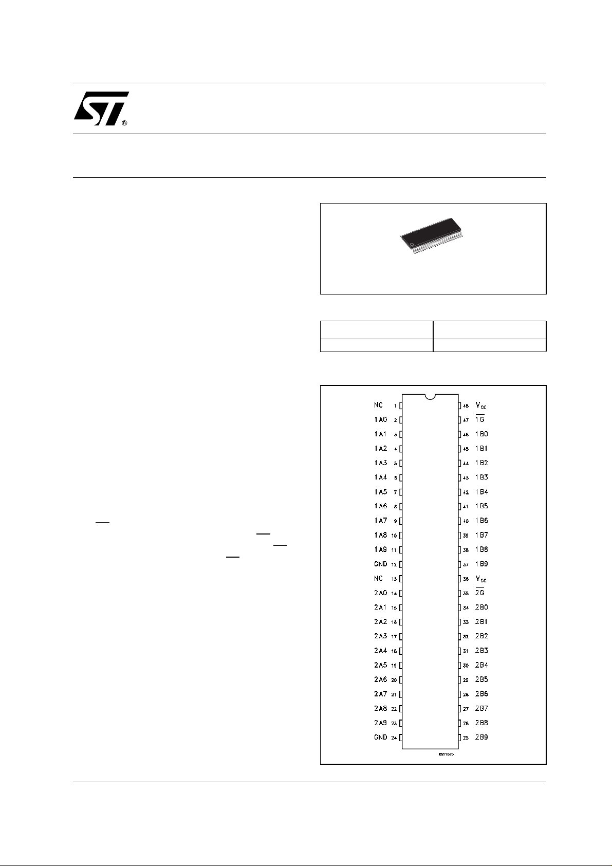
PIN CONNECTION
DESCRIPTION
The B5S16861 is an advanc ed high-speed CMOS
20-BIT TWO PORT BUS SWITCH fabricated with
sub-micron silicon gate and double-layer meta l
wiring C
It is ideal for 4V t o 5.5V V
2
MOS tecnology.
operations and
CC
ultra-low power and low noise applications,
typically notebook and docking station.
Any nG
SWITCHES. Output Enable inputs (nG
output control governs two 10-bit BUS
)tied
together gives full 20-bit operations. When nG
LOW, the switches are on. When nG
is HIGH, the
switches are in high impedance state.
It has ultra high-speed performanc e at 5V near
zero delay with low ON resistance.
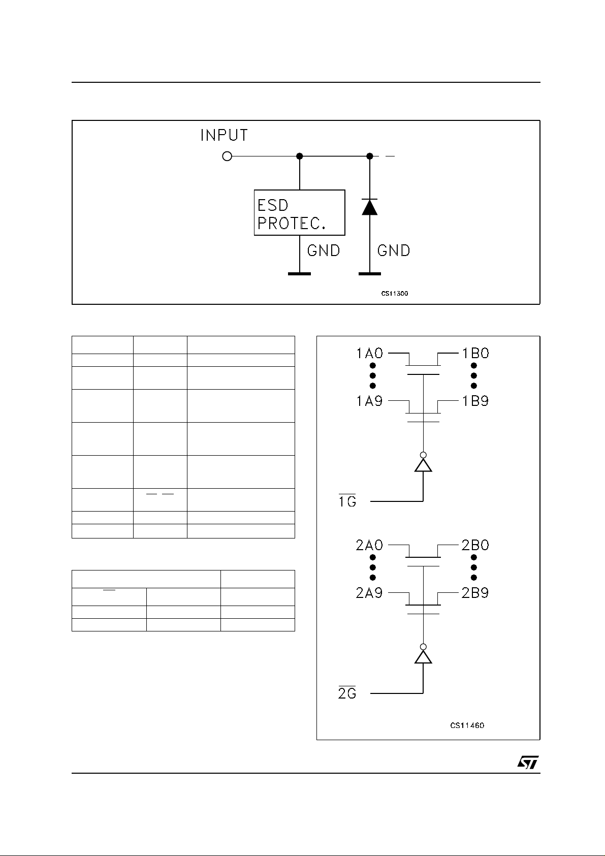
All inputs and outputs are equipped with protection circuits against st ati c discharge, giving them
2KV ESD immunity and transient excess vo ltage.
is
1/9February 2003
This is preliminary information on a new product now in development are or undergoing evaluation. Details subject to change without notice.
Page 2
B5S16861
INPUT EQUIVALENT CIRCUIT
PIN DESCRIPTION
PIN No SYMBOL NAME QND FUNCTION
1, 13 NC Not Connected
2, 3,4, 5,6,7,
8, 9, 10, 11
14,15,16,17,
18,19,20,21,
22, 23
34,33,32,31,
30,29,28,27,
26, 25
46,45,44,43,
42,41,40,39,
38, 37
47, 35 1G
12, 24 GND Ground (0V)
36, 48
1A0 to 1A9 Data Inputs
2A0 to 2A9 Data Inputs
2B0 to 2B9 Data Outputs
1B0 to 1B9 Data Outputs
,2G
V
CC
Bus Enable Input
(Active Low)
Positive Supply Voltage
TRUTH TABLE
INPUT OUTPUT
nG
L X Bus ON
HXZ
n:0to9
X: "H" or "L"
Z: HighImpedance
1An, 2An 1Bn, 2Bn
SCHEMATIC DIAGRAM
2/9
Page 3
B5S16861
ABSOLUTE MAXIMUM RATINGS
Symbol Parameter Value Unit
V
V
V
V
I
I
OK
I
or I
I
CC
T
T
Absolute Maximum Rating are those value beyond which damage to the device may occour. Functional operation under these condition is
not implied
1) IOabsolute maximum rating must be observed
2) V
<GND
O
3) Not more than one output should be tested at one time. Duration of the test should not exceed one second.
RECOMMENDED OPERATING CONDITIONS
Symbol Parameter Value Unit
V
V
V
V
T
dt/dv Switch Input Rise and Fall Time 0 to DC ns/V
dt/dv Control Input Rise and Fall Time (note 1) 0 to 10 ns/V
1) VINfrom0.8V to 2Vat VCC=3.0V
Supply Voltage
CC
DC Switch and Control Pin Voltage
I
DC Output Voltage (VCC= 0V) (note 1)
O
DC Output Voltage (V
O
DC Input Diode Current (V
IK
I/O
=Gnd)
I/O
< 0V)
DC Output Diode Current (note 2)
DC Output Current (note 3)
O
DC VCCor Ground Current per Supply Pin
GND
Storage Temperature
stg
Lead Temperature (10 sec)
L
Supply Voltage
CC
Input Voltage
I
Output Voltage (VCC= 0V)
O
Output Voltage 0 to 5.5
O
Operating Temperqture
op
-0.5 to +7.0 V
-0.5 to +7.0 V
-0.5 to +7.0 V
-0.5 to +7.0 V
-50 mA
-50 mA
128 mA
± 100 mA
-65 to +150 °C
300 °C
4 to 5.5 V
0 to 5.5 V
0 to 5.5 V
V
-55 to 125 °C
3/9
Page 4

B5S16861
DC SPECIFICATION
Test Condition Value
Symbol Parameter
V
V
V
R
I
V
I
I
CCD
OZ
CC
High Level Input Voltage
IH
Low Level Input Voltage
IL
Input Hysteresis at
H
Control pin
Switch ON Resistance
ON
I
Input Leakage Current
I
High Impedance Leakage
Current
Clamp Diode Voltage
IK
Quiescent Supply Current
Supply Current per
Control Input per MHz (1)
=25°C
T
V
CC
(V)
A
Min. Typ. Max. Min. Max. Min. Max.
4 to 5.5 2 2 2 V
4 to 5.5 0.8 0.8 0.8 V
4.5 to 5.5 150 mV
4.5
4.5
4.5
4.0
0 to 5.5
4.5 to 5.5
4.0 to 5.5
5.5
5.5
ION=64 mA
V
=0V
I
=48 mA
I
ON
V
=0V
I
=15 mA
I
ON
V
=2.4V
I
=15 mA
I
ON
V
=2.4V
I
VI= 5.5V or
GND
V
=5.5V
I/O
to GND
II= -18mA
VI=VCCor
GND
V
=Open
I/O
nG
=GND;
Control Input
Toggling
57
10 15
14 22
-0.7 -1.2 -1.2 V
0.1 1.0 3.0 10.0 µA
-40 to 85°C-55 to 125
°C
Unit
7
Ω
±0.1 ±1.0 ±2.0 µA
±1.0 ±2.0 µA
0.25
mA/
MHz
50% Duty
Cycle
∆I
CCICC
incr. per Input 5.5 VIC=VCC-2.1
2.5 mA
V
1) This current applies to the control inputs only and represent the current required to switch internal capacitance at the specified frequency.
The 1An and 2An inputs generate no significant AC or DC currents as they transition. This parameter is not tested, but is guaranteed by
design.
AC ELECTRICAL CHARACTERISTICS
Symbol Parameter
t
PLHtPHL
t
PZLtPZH
t
PLZtPHZ
1) Parameter guaranteed by design
2) X=1,2; n=0..9.
4/9
Propagation Delay Time (1)
xAn to xBn, xBn to xAn(2)
Output Enable Time
Output Disable Time
V
CC
(V)
4.5 to 5.5
Test Condition Value
-40 to 85 °C -55 to 125°C
C
(pF)
R
L
(Ω)
= t
t
L
s
r
(ns)
Min.Max.Min.Max.
50 500 2.5 0.25 ns
50 500 2.5 1.5 5.5 ns
50 500 2.5 1.5 5.5 ns
Unit
Page 5

CAPACITANCE CHARACTERISTICS
Symbol Parameter
C
C
Input Capacitance at Control
IN
Pin
Input Capacitance at I/O Pin
I/O
TEST CIRCUIT
Test Condition Value
V
CC
(V)
5.0
nG=V
CC
Min. Typ. Max.
B5S16861
=25°C
T
A
4pF
5.5 pF
Unit
TEST SWITCH
t
PLH,tPHL
t
PZL,tPLZ
t
PZH,tPHZ
CL= 50pF or equivalent (includes jig and probe capacitance)
RL=R1=500Ωor equivalent
RT=Z
of pulse generator (typically 50Ω)
OUT
Open
7V
Open
5/9
Page 6

B5S16861
WAVEFORM 1: PROPAGATION DELAY (f=1MHz; 50% duty cycle)
WAVEFORM 2: OUTPUT ENABLE AND DISABLE TIME (f=1MHz; 50% duty cycle)
6/9
Page 7

B5S16861
TSSOP48 MECHANICAL DATA
mm. inch
DIM.
MIN. TYP MAX. MIN. TYP. MAX.
A 1.2 0.047
A1 0.05 0.15 0.002 0.006
A2 0.9 0.035
b 0.17 0.27 0.0067 0.011
c 0.09 0.20 0.0035 0.0079
D 12.4 12.6 0.488 0.496
E 8.1 BSC 0.318 BSC
E1 6.0 6.2 0.236 0.244
e 0 .5 BSC 0.0197 BSC
K0˚ 8˚0˚ 8˚
L 0.50 0.75 0.020 0.030
A2
A
A1
b
e
D
K
c
E1
L
E
PIN 1 IDENTIFICATION
1
7065588C
7/9
Page 8

B5S16861
Tape & Reel TSSOP48 MECHANICAL DATA
mm. inch
DIM.
MIN. TYP MAX. MIN. TYP. MAX.
A 330 12.992
C 12.8 13.2 0.504 0.519
D 20.2 0.795
N 60 2.362
T 30.4 1.197
Ao 8.7 8.9 0.343 0.350
Bo 13.1 13.3 0.516 0.524
Ko 1.5 1.7 0.059 0.067
Po 3.9 4.1 0.153 0.161
P 11.9 12.1 0.468 0.476
8/9
Page 9

B5S16861
Information furnished is believed to be accurate and reliable. However, STMicroelectronics assumes no responsibility for the
consequences of use o f suc h inf ormat ion n or f or an y infr ingeme nt of paten ts or oth er ri gh ts of third part ies whic h may resul t f rom
its use. No license is granted by implication or otherwise under any patent or patent rights of STMicroelectronics. Specifications
mentioned in this publication are subject to change without notice. This publication supersedes and replaces all information
previously supplied. STMicroelectronics products are not authorized for use as critical components in life support devices or
systems without express written approval of STMicroelectronics.
Australia - Brazil - Canada - China - Finland - France - Germany - Hong Kong - India - Israel - Italy - Japan - Malaysia - Malta - Morocco
© The ST logo is a registered trademark of STMicroelectronics
© 2003 STMicroelectronics - Printed in Italy - All Rights Reserved
STMicroelectronics GROUP OF COMPANIES
Singapore - Spain - Sweden - Switzerland - United Kingdom - United States.
© http://www.st.com
9/9
 Loading...