

Page 1
Bay Linear, Inc
2418 Armstrong Street, Livermore, CA 94550 Tel: (925) 606-5950, Fax: (925) 940-9556 www.baylinear.com
100mA, µCap, Low Dropout Voltage Regulator
B5213
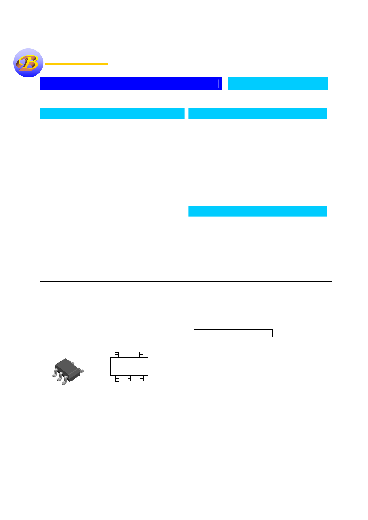
Smallest SC70
Pin Connection
Ordering Information
Package
SC70-5
B5213-XX
“XX” Voltage Selection Guide
Vout XX Code
2.8V
28
3.3V
33
3.0V
3
VEN
Logic High = Enabled
Logic Low = Shutdown
Description
The B5213 is a µCap, low dropout voltage regulator with very
low quiescent current, 220 µA typical, at 80mA load. It also
has very low dropout voltage, typically 20mV at light load and
330mV at 80mA. The B5213 provides up to 80mA and
consumes a typical of 1 µA in disable mode.
The B5213 is optimized to work with low value, low cost
ceramic capacitors. The output typically require only 0.47 µF
of output capacitance for stability. The enable pin can be tied
to V
IN
for easy device layout.
The B5213 is designed for portable, battery powered
equipment applications with small space requirements.
The B5213 is available in a space saving 5- pin SC70 package.
Performance is specified for the – 40 °C to + 125 °C
temperature range and is available in 2.8V, 3.0V and 3.3V
fixed voltages. For other output voltage options, please contact
Bay Linear.
Features
• Output Current 100mA
•
Space Saving SC70
• 2.8.0V, 3.3V and 3.0V Versions
• Very Low Quiescent Current
•
Low Dropout Voltage
•
Very Low Temperature Coefficient
•
Needs only 1µF for Stability
•
Error Flag warns of output dropout
•
Logic-Controlled Electronic Shutdown
•
Pin-to-Pin MIC5213
Applications
• Battery Powered Systems
• Portable instrumentation
• Notebooks Computers
• Potable Consumer Equipment
• Bar Code Scanner
• Cellular Phones
Bay Linear
Inspire the Linear Power
SC-70 (L5)
Top View
GND
V
EN
NC
32
1
45
V
IN
V
OUT
SC-70 (L5)
Top View
GND
V
EN
NC
32
1
45
V
IN
V
OUT
Page 2
Bay Linear, Inc
2418 Armstrong Street, Livermore, CA 94550 Tel: (925) 606-5950, Fax: (925) 940-9556 www.baylinear.com
B5213
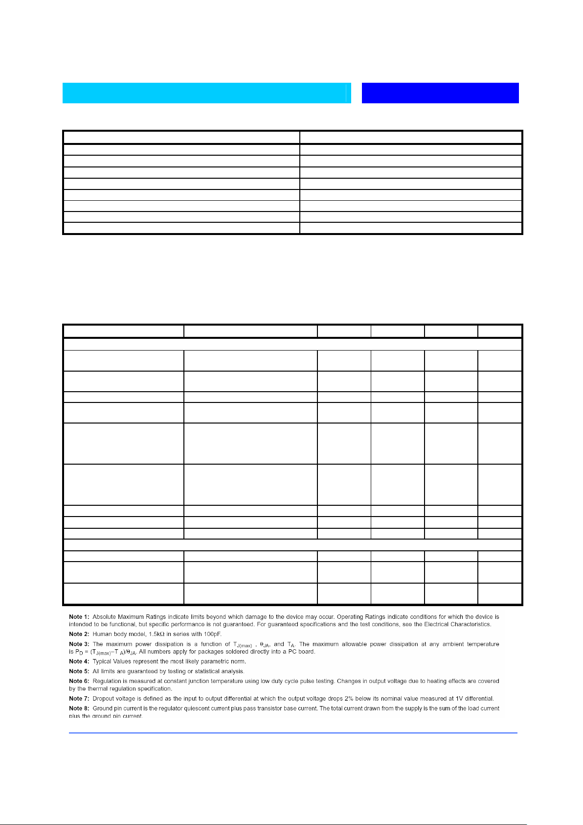
Absolute Maximum Rating
Parameter
Power Dissipation Internally Limited
Lead Temperature ( Soldering 5 seconds )
260 °C
Storage Temperature Range
-65 °C to +150 °C
Operating Junction Temperature
-40 °C to +125 °C
Input Supply Voltage 2.7V to 6V
V
EN
0V to V
IN
Shutdown Input Voltage -0.3V to +30V
Package Thermal Resistance
478°C
Electrical Characteristics
Unless otherwise specified, all limits guaranteed for TJ = 25 °C, VIN = V
OUT
+ 1V, IL = 1mA, CL = 0.47 µF, VEN ≥
2.0V. Boldface limits apply at the temperature extremes.
Parameter Conditions MIN TYP MAX UNIT
Output Voltage -3
-4
3 4 %
Output Voltage Temperature
Coefficient
(Note 10) 50 200
ppm / ° C
Line Regulation VIN = V
OUT
+1V to 6V
0.008 0.3 %
Load Regulation IL=0.1mA to 80mA (Note 6) 0.08 0.3
0.5
%
Dropout Voltage (Note 7)
I
L
= 100µA
I
L
= 20mA
I
L
= 50mA
I
L
= 80mA
20
70
180
330
350
600
mV
Ground pin Current
I
L
= 100µA, VEN≥2.0V(active)
I
L
= 20mA, VEN≥2.0V(active)
I
L
= 500mA, VEN≥2.0V(active)
I
L
= 80mA, VEN≥2.0V(active)
160
180
200
220
750
3000
µA
Ground pin Current at Dropout VIN=V
OUT(NOMINAL)-
0.5V Note (8) 200 300
µA
Quiescent Current VEN≤0.4V(Shutdown) 110 170
µA
Current Limit V
OUT
= 0 180 250 mA
Enable Input
Thermal Regulation (Note 9) 0.05 % / W
Enable Input Voltage Level VIL, logic Low (off)
V
IH
, Logic High (on)
2.0
0.6
µA
Enable Input Current VEN≤0.4V
V
IH
≥2.0V
0.01
15
1
50
µA
Page 3

Bay Linear, Inc
2418 Armstrong Street, Livermore, CA 94550 Tel: (925) 606-5950, Fax: (925) 940-9556 www.baylinear.com
B5213
Page 4

Bay Linear, Inc
2418 Armstrong Street, Livermore, CA 94550 Tel: (925) 606-5950, Fax: (925) 940-9556 www.baylinear.com
B5213
APPLICATION HINTS
The B5213 is a low dropout, linear regulator
designed primarily for battery- powered applications.
The B5213 can be used with low cost ceramic
capacitors, typical value of 0.47 µF.
As illustrated in the simplified schematics, the B5213
consists of a 1.25V reference, error amplifier, Pchannel pass transistor and internal feedback voltage
diode. The 1.25V reference is connected to the input
of the error amp. The error amp compares this
reference with the feedback voltage. If the feedback
voltage is lower than the reference, the pass transistor
gate is pulled lower allowing more current to pass
and increasing the output voltage. If the feedback
voltage is too high, the pass transistor gate is pulled
up allowing less current to pass to the output. The
output voltage is feedback through the resistor
divider. Additional blocks include short circuit
current protection and thermal protection.
The B5213 features an 80mA P- channel MOSFET
transistor. This provides several advantages over
similar designs using PNP pass transistors including
longer battery life.
The P- channel MOSFET requires no base drive,
which reduces quiescent current considerably. PNP
based regulators waste considerable amounts of
current in dropout when the pass transistor saturates.
They also have high base drive currents under large
loads. The B5213 does not suffer from these
problems and consumes only the specified quiescent
current under light and heavy loads.
External Capacitors
Like any low- dropout regulators, the B5213 requires
external capacitors for regulator stability. The B5213
is specially designed for portable applications
requiring minimum board space and the smallest
components.
A 0.1µF capacitor should be placed from V
IN
to
GND if there is more than 10 inches of wire between
the input and AC filter or when a battery is used as
the input. This capacitor must be
Located a distance of not more than 1cm from the
input pin and returned to a clean analog ground.
The B5213 is designed to work with small ceramic
output capacitors. Ceramic capacitors ranging between
0.47 µF to 4.7 µF are the smallest and least expensive.
No- Load Stability
The B5213 will remain stable and in regulation with
no- load (other than the internal voltage divider). This
is especially important in CMOS RAM keep- alive
applications.
Enable Input
The B5213 is shut off by pulling the VEN pin below
0.6V; all internal circuitry is powered off and the
quiescent current is typically 1 µA. Pulling the V
EN
high above 2V re- enables the device and allows
operation. If the shut down feature is not used, the V
EN
pin should be tied to V
IN
to keep the regulator output
on all the time.
Thermal Behavior
The B5213 regulator has internal thermal shutdown to
protect the device from over heating. Under all
operating conditions, the maximum junction
temperature of the B5213 must be below 125 °C.
Maximum power dissipation can be calculated based
on the output current and the voltage drop across the
part. The maximum power dissipation is
P
D( MAX)
= ( T
J( MAX)
- TA)/ φ
JA
φ
JA
is the junction- to- ambient thermal resistance, 478
°C/ W for the B5213 in the SC70 package. T
A
is the
maximum ambient temperature T
J( MAX)
is the
maximum junction temperature of the die, 125 °C
When operating the B5213 at room temperature, the
maximum power dissipation is 209mW.
The actual power dissipated by the regulator is
PD = ( V
IN
- V
OUT
) IL + VIN I
GND
The figure below shows the voltage and currents,
which are present in the circuit.
Page 5

Bay Linear, Inc
2418 Armstrong Street, Livermore, CA 94550 Tel: (925) 606-5950, Fax: (925) 940-9556 www.baylinear.com
B5213
B5213
B5213
Page 6

Bay Linear, Inc
2418 Armstrong Street, Livermore, CA 94550 Tel: (925) 606-5950, Fax: (925) 940-9556 www.baylinear.com
Advance Information- These data sheets contain descriptions of products that are in development. The specifications are based on the engineering calculations,
computer simulations and/ or initial prototype evaluation.
Preliminary Information- These data sheets contain minimum and maximum specifications that are based on the initial device characterizations. These limits are
subject to change upon the completion of the full characterization over the specified temperature and supply voltage ranges.
The application circuit examples are only to explain the representative applications of the devices and are not intended to guarantee any circuit
design or permit any industrial property right to other rights to execute. Bay Linear takes no responsibility for any problems related to any
industrial property right resulting from the use of the contents shown in the data book. Typical parameters can and do vary in different
applications. Customer’s technical experts must validate all operating parameters including “ Typical” for each customer application.
LIFE SUPPORT AND NUCLEAR POLICY
Bay Linear products are not authorized for and should not be used within life support systems which are intended for surgical
implants into the body to support or sustain life, in aircraft, space equipment, submarine, or nuclear facility applications without
the specific written consent of Bay Linear President.
 Loading...