

Page 1
Bay Linear
Bay Linear
Bay LinearBay Linear
Inspire the Linear Power
Inspire the Linear Power
Inspire the Linear PowerInspire the Linear Power
1.24V Adjustable Shunt Regulator
B431L
Description
The B431L is a three terminal adjustable shunt regulator with
thermal stability of 50ppm/°C. The output voltage can be
adjusted to any value from 1.24V (V
external resistors. These devices have a typical output
impedance of 0.05Ω. Active output circuitry provides a very
sharp turn-on characteristics and making the device excellent
replacement for zener diodes in many applications. The B431L
is an ideal voltage reference in an isolated feedback circuit for
3.0V switch mode power supplies
The B431L shunt regulator is available with three voltage
tolerances (0.5%, 1.0% and 2.0%) and three package options
(SOT-23-3, TO-92, 8SOIC). This allows the designer the
opportunity to select the optimum combination of cost and
performance for their application.
) to 16V with two
REF
Features
• Low voltage operation (down to 1.24V)
• Wide operating current……80µA to 100mA
• Trimmed bandgap design………….. ± 0.5%
• Low Dynamic Output Impedance…....0.05ΩΩΩΩ
• Wide temperature range…... -40°°°°C to +85°°°°C
Available in ….….SOT-23-3, TO-92 , 8SOIC
•
Pin-to-Pin Replacement …………….SC431L
•
Applications
• Switching Power Supplies
• Adjustable Power Supplies
• Linear Regulators
• Battery Powered Equipment
• Monitors, TV, VCR
• Instrumentation
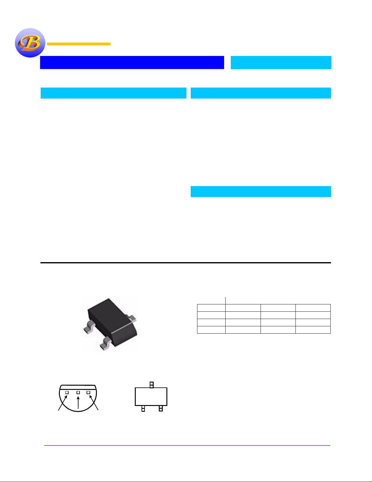
Pin Connection
Ordering Information
Package Tolerance
0.5% 1% 2%
TO-92 B431LAZ B431LBZ B431LCZ
SO-8 B431LAM B431LBM B431LCM
SOT-23 B431LAK3 B431LBK3 B431LCK3
TO-92 (Z)
TO-92 (Z)
2
2
13
13
SOT-23-3 (K3)
SOT-23-3 (K3)
Anode
Anode
BAY
BAY
Ref
Ref
Bay Linear, Inc
Anode
Anode
Bottom View
Bottom View
Cathode
Cathode
2418 Armstrong Street, Livermore, CA 94550 Tel: (925) 606-5950, Fax: (925) 940-9556 www.baylinear.com
Ref
Ref
Top View
Top View
Cathode
Cathode
Page 2
B431L
Absolute Maximum Rating
Parameter Symbol Maximum Units
Cathode Voltage Vz 20 V
Continuous Cathode Current Iz 100 mA
Reference Input Current Range 3 mA
Power Dissipation at TA - 25°C
SOT-23-3
S0-8
TO-92
Thermal Resistance
SOT-23-3
S0-8
TO-92
P
D
O
JA
0.37
0.75
0.95
336
175
132
Operating Junction Temperature Range TJ -40 to +150
Storage Temperature Range T
Lead Temperature (Soldering) 10 seconds T
ESD Rating (Human Body Model) T
Recommended Operating Con ditions
-65 to +150
STG
300
LEAD
2 kV
ESD
W
°
C/W
°
°
°
C
C
C
Min Max Symbol
Cathode Voltage, Vz V
Cathode Current, Iz 80µA 100 mA
16 V
REF
Electrical Characteristics
Unless specified: T
. Values in bold apply over full operating ambient temperature.
٨ = 25°C
Parameter Symbol Condition Min Typ Max Units
V
Temp Deviation V
REF
V
REF
V
DEV
Z
Z
= V
= V
REF1 IZ
REF1, IZ
= 10mA
= 10mA
IA=full range
Ratio of Change in
V
To Change in V
REF
Reference Input
Current
I
Temperature
REF
Deviation
Off-State Cathode
Current
Z
Δ V
ΔVZ
I
REF
I
REF(DEV)
I
Z (OFF)
REF
= 10mA,ΔV
I
Z
= 16V to V
Z
(2)
R1 = 10kΩ, R2 = ∞,
I
= 10mA
Z
R1 = 10kΩ, R2 = ∞,
I
= 10mA
Z
V
= 0V, VZ =16V
REF
V
= 0V, VZ =16V
REF
Min Operating
I
V
Z(MIN)
= V
Z
REF
Current
Dynamic Impedance Z
KA
I
=100µA to 100mA, f≤1kHA
K
VKA=V
ref
(1)
1.234 1.246 Reference Voltage V
1.222
(1)
Ref
(2)
(2)
(3)
(3)
(1)
20 80 µA
,
10 25 mV
-2.7 -1.0 mV/V
0.15 0.5
0.1 0.4
0.125 0.150
0.135 0.150
0.05 0.15
B431LA 0.5%
1.240
1.258
V
µ
A
µ
A
µA
Ω
Bay Linear, Inc
2418 Armstrong Street, Livermore, CA 94550 Tel: (925) 606-5950, Fax: (925) 940-9556 www.baylinear.com
Page 3
B431L
Electrical Characteristics
Unless specified: T
. Values in bold apply over full operating ambient temperature.
٨ = 25°C
Parameter Symbol Condition Min Typ Max Units
V
Temp Deviation V
REF
V
REF
V
DEV
Z
Z
= V
= V
REF1 IZ
REF1, IZ
= 10mA
= 10mA
IA=full range
Ratio of Change in
V
To Change in V
REF
Reference Input
Current
I
Temperature
REF
Deviation
Off-State Cathode
Current
Z
Δ V
ΔVZ
I
REF
I
REF(DEV)
I
Z (OFF)
REF
= 10mA,ΔV
I
Z
= 16V to V
Z
(2)
R1 = 10kΩ, R2 = ∞,
I
= 10mA
Z
R1 = 10kΩ, R2 = ∞,
I
= 10mA
Z
V
= 0V, VZ =16V
REF
V
= 0V, VZ =16V
REF
Min Operating
I
V
Z(MIN)
= V
Z
REF
Current
Dynamic Impedance Z
KA
I
=100µA to 100mA, f≤1kHA
K
VKA=V
ref
(1)
1.228 1.252 Reference Voltage V
1.215
(1)
Ref
(2)
(2)
(3)
(3)
(1)
20 80 µA
,
10 25 mV
-1.0 -2.7 mV/V
0.15 0.5
0.1 0.4
0.125 0.150
0.135 0.150
0.05 0.15
B431LB 1%
1.240
1.265
V
µ
A
µ
A
µA
Ω
Electrical Characteristics
Unless specified: T
. Values in bold apply over full operating ambient temperature.
٨ = 25°C
Parameter Symbol Condition Min Typ Max Units
V
Temp Deviation V
REF
V
REF
V
DEV
Z
Z
= V
= V
REF1 IZ
REF1, IZ
= 10mA
= 10mA
IA=full range
Ratio of Change in
V
To Change in V
REF
Reference Input
Current
I
Temperature
REF
Deviation
Off-State Cathode
Current
Z
Δ V
ΔVZ
I
REF
I
REF(DEV)
I
Z (OFF)
REF
= 10mA,ΔV
I
Z
= 16V to V
Z
(2)
R1 = 10kΩ, R2 = ∞,
I
= 10mA
Z
R1 = 10kΩ, R2 = ∞,
I
= 10mA
Z
V
= 0V, VZ =16V
REF
V
= 0V, VZ =16V
REF
Min Operating
I
V
Z(MIN)
= V
Z
REF
Current
Dynamic Impedance Z
KA
I
=100µA to 100mA, f≤1kHA
K
VKA=V
ref
(1)
1.215 1.265 Reference Voltage V
1.200
(1)
Ref
(2)
(2)
(3)
(3)
(1)
20 80 µA
,
10 35 mV
-1.0 -2.7 mV/V
0.15 0.5
0.1 0.4
0.125 0.150
0.135 0.150
0.05 0.15
B431LC 2%
1.240
1.280
V
µ
A
µ
A
µA
Ω
Bay Linear, Inc
2418 Armstrong Street, Livermore, CA 94550 Tel: (925) 606-5950, Fax: (925) 940-9556 www.baylinear.com
Page 4

B431L
Bay Linear, Inc
2418 Armstrong Street, Livermore, CA 94550 Tel: (925) 606-5950, Fax: (925) 940-9556 www.baylinear.com
Page 5

B431L
Test Circuit: Small-Signal Gain & Phase
43
Test Circuit: Stability
431
Bay Linear, Inc
2418 Armstrong Street, Livermore, CA 94550 Tel: (925) 606-5950, Fax: (925) 940-9556 www.baylinear.com
Page 6

Application Notes:
B431L
B431
Stability:
Selection of load capacitor for when B431L is used as a
shunt regulator, two options for selection of C
load capacitance across the device, decouple at the load
2) Large capacitance across the device, optional
decoupling at the load.
The reason for this is that B431L exhibits instability
with capacitances in the range of 10nF to 1µF (approx.)
at light cathode currents (up to 3mA typical). The
device is less stable the lower the cathode voltage has
been set for. Therefore while the device will be
perfectly stable operating at a cathode current of 10mA
with a 0.1µF capacitor across it, it will oscillate
transiently during start-up as the cathode current passes
through the instability region. Selecting a very low (or
preferably, no) capacitance, or alternatively a high
capacitance such as 10µF will avoid this issue
altogether. Since the user anyway, the most cost
effective method is to use no capacitance at all directly
across the device. PCB trace/via resistance and
inductance prevent the local load decoupling from
causing the oscillation during the transient start-up
phase.
Note: if the B431L is located right at the load, so the
load decoupling capacitor is directly across it, then this
capacitor will have to be ≤1nF or ≥ 10µF
Selection of Load Capacitor
1) No
L
Bay Linear, Inc
2418 Armstrong Street, Livermore, CA 94550 Tel: (925) 606-5950, Fax: (925) 940-9556 www.baylinear.com
Page 7

Test Circuits:
Application Circu it:
+12V
B431L
+3.3V
470µF0.1µF
PHD 3055E
500Ω
Ω
0.1µF
0.1µF
B431L
*If the output voltage has noise, then please add a 0.1µF in between drain and gate of power MOSFET to
reduce the noise.
Bay Linear, Inc
2418 Armstrong Street, Livermore, CA 94550 Tel: (925) 606-5950, Fax: (925) 940-9556 www.baylinear.com
140
120
Ω
2.7V
0.1µF
INTEL
I 740
1000µF
Page 8

B431L
SOT-23
0.015 - 0.018
(0.381 - 0.457)
0.047 - 0.055
(1.194 - 1.397)
0.083 - 0.098
(2.108 - 2.489)
0.020 - 0.024
(0.508 - 0.610)
0.035 - 0.040
(0.889 - 1.016)
0.070 - 0.080
(1.778 - 2.032)
0.110 - 0.120
(2.794 - 3.048)
0.003 - 0.005
(0.076 - 0.127)
0.001 - 0.004
(0.025 - 0.102)
0.030 - 0.041
(0.762 - 1.041)
0.018 - 0.024
(0.457 - 0.610)
Advance Information
computer simulations and/ or initial prototype evaluation.
-
These data sheets contain descriptions of products that are in development. The specifications are based on the engineering calculations,
-
Preliminary Information
subject to change upon the completion of the full characterization over the specified temperature and supply voltage ranges.
These data sheets contain minimum and maximum specifications that are based on the initial device characterizations. These limits are
The application circuit examples are only to explain the representative applications of the devices and are not intended to guarantee any circuit
design or permit any industrial property right to other rights to execute. Bay Linear takes no responsibility for any problems related to any
industrial property right resulting from the use of the contents shown in the data book. Typical parameters can and do vary in different
applications. Customer’s technical experts must validate all operating parameters including “ Typical” for each customer application.
LIFE SUPPORT AND NUCLEAR POLICY
Bay Linear products are not authorized for and should not be used within life support systems which are intended for surgical
implants into the body to support or sustain life, in aircraft, space equipment, submarine, or nuclear facility applications without
the specific written consent of Bay Linear President.
Bay Linear, Inc
2418 Armstrong Street, Livermore, CA 94550 Tel: (925) 606-5950, Fax: (925) 940-9556 www.baylinear.com
 Loading...