

Page 1
h
Bay Linear
Inspire the Linear Power
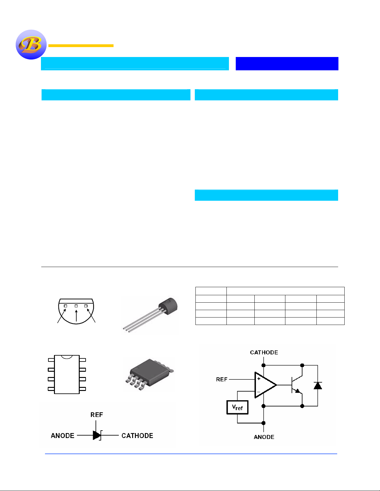
2.5V Adjustable Shunt Regulator
Description
The Bay Linear B431 is a three terminal adjustable shunt
regulator with thermal stability over Temperature range. Using
two external resistors allows the output voltage to be adjusted
from 2.5V to 36V. With a sharp turn on characteristics the
B431 a superior replacement for zener diode applications.
The B431 shunt regulator has a tolerance of 0.5% which has
proven to be sufficient to overcome all of the other errors in
the system to virtually eliminate the need for trimming in the
power supply manufacturers assembly line and contribute a
significant cost savings.
Features
• Wide Operating Range …1mA to100mA
• Tight Band Gap Tolerance …….… 0.5%
• Low Temp. Coefficient………..30 ppm/
• Wide temp range of –40 to +105
• Available in TO92, SOT-89, SO-8
Applications
• Switching Power Supplies
• Adjustable Power Supplies
• Linear Regulators
• Battery Powered Equipment
• Monitors, TV, VCR
• Instrumentation
Package Information Ordering Information
Ref
TO-92 (Z)
132
Anode
Bottom View
Cat
Package Tolerance
0.5% 1% 1% 2%
TO-92
SOT-89
8SOIC
The Electrical Grade & Type is specified on shipping Box Only
B431AZ B431BZ B431DBZ B431CZ
B431AR B431BR B431DBR B431CR
B431AM B431BM B431DBM B431CM
8-Pin Surface Mount (M)
B431
o
C
o
C
1
2
3
4
Top View
8
7
6
5
Bay Linear, Inc
2418 Armstrong Street, Livermore, CA 94506 Tel: (925) 606-5950, Fax: (925) 940-9556 www.baylinear.com
Page 2
B431
Absolute Max Ratings
Parameter Symbol Maximum Units
Cathode Voltage Vz 37 V
Continuous Cathode Current Iz 150 mA
Reference Input Current I
Power Dissipation at TA - 25°C
SOT-89
S0-8
TO-92
Thermal Resistance
S0-8
TO-92
SOT-89
Operating Junction Temperature Range TJ -40 to +150
Operating Ambient Temperature T
Storage Temperature Range T
Lead Temperature (Soldering) 10 seconds T
ESD Rating (Human Body Model) T
10 mA
REF
P
D
O
JA
1000
750
775
175
160
110
mW
°C/W
°C
A
-65 to +150
STG
300
LEAD
2 kV
ESD
-40 to +105
°C
°C
°C
Recommended Operating Conditions
Cathode Voltage, Vz V
Cathode Current, Iz 0.1 100 mA
Min Max Symbol
36 V
REF
Electrical Characteristics
Unless specified: T
Parameter Symbol Condition Min Typ Max Units
Reference Voltage V
V
Temp Deviation V
REF
Ratio of Change in
V
To Change in V
REF
Reference Input
Current
I
Temperature
REF
Deviation
Off-State Cathode
Current
Dynamic Output
Impedance
Minimum Operating
Current
. Values in bold apply over full operating ambient temperature.
٨ = 25°C
(1)
(1)
2.483 2.495 2.507 V
4 17 mV
Ref
-1.0 -2.7
-0.4 -2.0
(2)
(2)
(3)
0.1 1
= V
REF
(1)
(1)
0.4 1 mA
0.7 4
0.4 1.2
0.20 0.50
Z
V
REF
V
DEV
∆ V
REF
∆VZ
IREF
I
REF(DEV)
I
V
Z (OFF)
rz
I
V
Z(MIN)
= V
Z
= V
Z
IZ = 10mA,∆V
I
= 10mA,∆V
Z
R1 = 10kΩ, R2 = ∞,
R1 = 10kΩ, R2 = ∞,
REF
F <1kHz, V
I
= 1mA to 100mA
Z
= 10mA
REF1 IZ
= 10mA
REF1 IZ
= 10V to V
Z
= 36V to 10V
Z
I
= 10mA
Z
= 10mA
I
Z
= 0V, VZ =36V
Z
= V
Z
REF
B431 0.5%
mV/V
µA
µA
µA
Ω
Bay Linear, Inc
2418 Armstrong Street, Livermore, CA 94506 Tel: (925) 606-5950, Fax: (925) 940-9556 www.baylinear.com
Page 3
B431
Parameter Symbol Condition Min Typ Max Units
Reference Voltage V
V
Temp Deviation V
REF
Ratio of Change in
V
To Change in V
REF
Z
Reference Input
Current
I
Temperature
REF
Deviation
Off-State Cathode
Current
Dynamic Output
Impedance
Minimum Operating
Current
V
REF
V
DEV
∆ V
REF
∆VZ
IREF
I
REF(DEV)
I
V
Z (OFF)
rz
I
V
Z(MIN)
= V
Z
= V
Z
IZ = 10mA,∆V
I
= 10mA,∆V
Z
R1 = 10kΩ, R2 = ∞,
R1 = 10kΩ, R2 = ∞,
REF
F <1kHz, V
I
= 1mA to 100mA
Z
= 10mA
REF1 IZ
= 10mA
REF1 IZ
= 10V to V
Z
= 36V to 10V
Z
I
= 10mA
Z
= 10mA
I
Z
= 0V, VZ =36V
Z
= V
Z
REF
(1)
(1)
2.470 2.495 2.520 V
4 17 mV
Ref
-1.0 -2.7
-0.4 -2.0
(2)
(2)
(3)
0.1 1
= V
REF
(1)
(1)
0.4 1 mA
0.7 4
0.4 1.2
0.20 0.50
B431 1%
mV/V
µA
µA
µA
Ω
Parameter Symbol Condition Min Typ Max Units
Reference Voltage V
V
Temp Deviation V
REF
Ratio of Change in
V
To Change in V
REF
Z
Reference Input
Current
I
Temperature
REF
Deviation
Off-State Cathode
Current
Dynamic Output
Impedance
Minimum Operating
Current
V
REF
V
DEV
∆ V
REF
∆VZ
IREF
I
REF(DEV)
I
V
Z (OFF)
rz
V
I
Z(MIN)
= V
Z
= V
Z
IZ = 10mA,∆V
I
= 10mA,∆V
Z
R1 = 10kΩ, R2 = ∞,
R1 = 10kΩ, R2 = ∞,
REF
F <1kHz, V
I
= 1mA to 100mA
Z
= 10mA
REF1 IZ
= 10mA
REF1 IZ
= 10V to V
Z
= 36V to 10V
Z
I
= 10mA
Z
= 10mA
I
Z
= 0V, VZ =36V
Z
= V
Z
REF
(1)
(1)
2.445 2.495 2.545 V
4 17 mV
Ref
-1.0 -2.7
-0.4 -2.0
(2)
(2)
(3)
0.1 1
= V
REF
(1)
(1)
0.4 1 mA
0.7 4
0.4 1.2
0.20 0.50
B431 2%
mV/V
µA
µA
µA
Ω
Bay Linear, Inc
2418 Armstrong Street, Livermore, CA 94506 Tel: (925) 606-5950, Fax: (925) 940-9556 www.baylinear.com
Page 4
B431
Parameter Symbol Condition Min Typ Max Units
Reference Voltage V
V
Temp Deviation V
REF
Ratio of Change in
V
To Change in V
REF
Z
Reference Input
Current
I
Temperature
REF
Deviation
Off-State Cathode
Current
Dynamic Output
Impedance
Minimum Operating
Current
V
REF
V
DEV
∆ V
REF
∆VZ
IREF
I
REF(DEV)
I
V
Z (OFF)
rz
I
V
Z(MIN)
= V
Z
= V
Z
IZ = 10mA,∆V
I
= 10mA,∆V
Z
R1 = 10kΩ, R2 = ∞,
R1 = 10kΩ, R2 = ∞,
REF
F <1kHz, V
I
= 1mA to 100mA
Z
= 10mA
REF1 IZ
= 10mA
REF1 IZ
= 10V to V
Z
= 36V to 10V
Z
I
= 10mA
Z
= 10mA
I
Z
= 0V, VZ =36V
Z
= V
Z
REF
Note 1: B431D is rated at -40°C to +85°C and 50ppm/°C
(1)
(1)
2.470 2.495 2.520 V
4 17 mV
Ref
-1.0 -2.7
-0.4 -2.0
(2)
(2)
(3)
0.1 1
= V
REF
(1)
(1)
0.4 1 mA
0.7 4
0.4 1.2
0.20 0.50
B431D 1%
mV/V
µA
µA
µA
Ω
Bay Linear, Inc
2418 Armstrong Street, Livermore, CA 94506 Tel: (925) 606-5950, Fax: (925) 940-9556 www.baylinear.com
Page 5

Calculating Average Temperature Coefficient (TC)
5000
ppm
0.5
Test Circuit
V
IN
I
REF
Figure
mV
%
000
-10
-20
-55
-25 0 25 50 75 100 125
0.06 mV/°C
0.002 %/°C
24 ppm/°C
I
1a. Test Circuit 1
∆
V
REF
Temperature (°C)
V
= V
KA
REF
K
∆Τ
V
IN
R
1
(V
)
REF
R
2
Figure
1b. Test Circuit 2
TC in mV/°C =
TC in %/°C =
TC in ppm/°C =
V
KA
I
K
∆
V
REF
∆
)
∆
V
at 25°C
V
REF
∆
)
∆
V
REF
V
IN
Figure
1c. Test Circuit 3
(mV)
T
A
REF
T
A
V
REF
at 25°C
∆
T
A
B431
x 100
)
)
I
K (OFF)
x 10
V
KA
6
Bay Linear, Inc
2418 Armstrong Street, Livermore, CA 94506 Tel: (925) 606-5950, Fax: (925) 940-9556 www.baylinear.com
Page 6

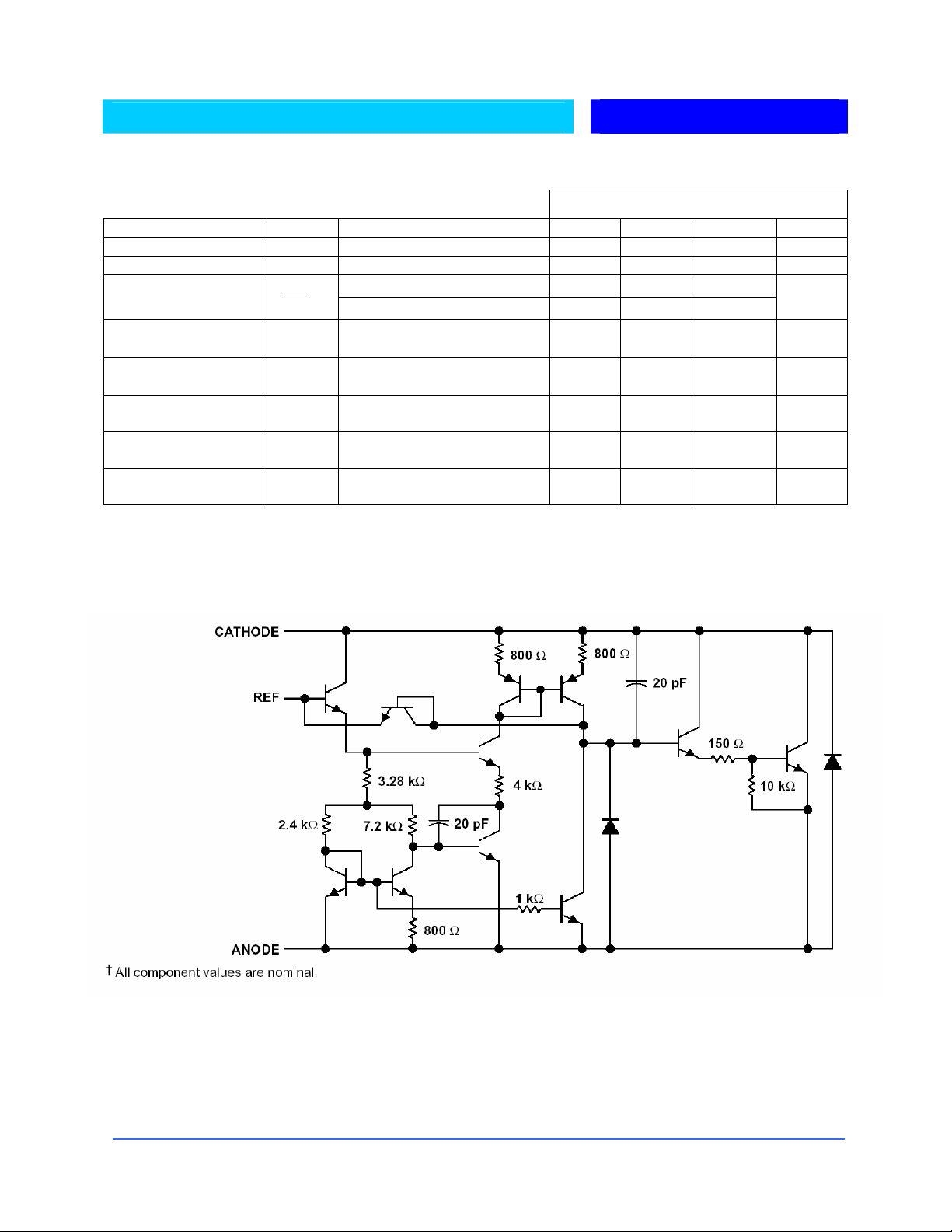
TYPICAL PERFORMANCE CURVES
B431
A)
µ
- Cathode Current (
K
I
-100
-200
100
900
800
700
600
500
400
300
200
100
0
VKA = 18V
V
REF
10
1
Low Current Operating Characteristics
VKA = V
Temperature Range: - 0 to 105 °C
REF
105 °C
25 °C
-0°C
1.0-1.0 2.00
VKA - Cathode Voltage (V)
Figure 2
Off State Leakage
= 0V
High Current Operating Characteristics
150
VKA = V
125
100
)
A
m
(
t
n
e
r
r
u
C
e
d
o
h
t
a
C
-
K
I
-100
3.0
Temperature Range: - 0 to 105 °C
75
50
25
0
-25
-50
-75
-2-10123
REF
VKA - Cathode Voltage (V)
Figure 3
2.53
2.52
)
V
(
2.51
e
g
a
t
l
o
V
2.50
e
c
n
e
r
e
f
e
2.49
R
-
F
E
R
V
2.48
Reference Voltage vs. Ambient Temperature
VKA = V
REF
IK = 10 mA
= 2.500 V at 25 °C
V
REF
off - Off State Cathode Current (nA)
0.1
Z
I
0.01
-60 -30 0 30 60 90 120
TA - Ambient Temperature ( °C)
Figure 4
Bay Linear, Inc
2418 Armstrong Street, Livermore, CA 94506 Tel: (925) 606-5950, Fax: (925) 940-9556 www.baylinear.com
2.47
2.46
2.45
-60 -30 0 30 60
TA - Ambient Temperature ( °C)
Figure 5
90 120
Page 7

TYPICAL PERFORMANCE CURVES
B431
3.0
)
2.5
A
(
µ
t
n
e
r
r
2.0
u
C
t
u
p
n
1.5
I
e
c
n
e
r
e
f
1.0
e
R
-
F
E
R
I
0.5
0
-60 -30 0 30 60 90 120
Reference Input Current
R1 = 10 k
R2 =
IK = 10 mA
TA - Ambient Temperature ( °C)
Figure 6
Noise Voltage
Hz
√
70
60
50
40
30
Noise Voltage nV/
20
10
VKA = V
REF
IK = 10 mA
T
= 25°C
A
0
10 100 1 k 10 k 100 k
f - Frequency (Hz)
Figure 8
0
Ω
∞
-10
-20
-30
- Change in Reference Voltage (mV)
-40
REF
V
-50
Reference Voltage Line Regulation
0 °C
25 °C
75 °C
- Cathode Voltage (V)
V
KA
105 °C
180 3 6 9 12 15
Figure 7
0.150
0.125
)
Ω
0.100
(
e
c
n
a
d
e
p
0.075
m
I
c
i
m
a
n
0.050
y
D
-
A
K
Z
0.025
0.0
-60 -30 0 30 60 90 120
Low Frequency Dynamic Output Impedance
= V
V
KA
REF
IKA = 1 to 100 mA
1 kHz
f <
TA - Free Air Temperature
Figure 9
Bay Linear, Inc
2418 Armstrong Street, Livermore, CA 94506 Tel: (925) 606-5950, Fax: (925) 940-9556 www.baylinear.com
Page 8

TYPICAL PERFORMANCE CURVES
B431
100
10
1.0
- Dynamic Impedance
KA
Z
0.1
0.01
1 k 10 k 100 k 1 M
Small Signal Voltage Gain vs. Frequency
70
Temperature Range: -0 to 105 °C
60
50
40
30
TA = 25 °C
= 1 to 100 mA
I
K
I
= 10 mA
K
Dynamic Output Impedance
f - Frequency (Hz)
Figure 10
9 µF
15 k
10 M
OUT
Ω
I
K
230
20
- Small Signal Voltage Gain (dB)
V
A
10
0
1 k 10 k 100 k 1 M 10 M
Bay Linear, Inc
8.25 k
GND
f - Frequency (Hz)
Figure 11
2418 Armstrong Street, Livermore, CA 94506 Tel: (925) 606-5950, Fax: (925) 940-9556 www.baylinear.com
Page 9

TYPICAL PERFORMANCE CURVES
B431
6
5
4
3
2
1
Input and Output Voltages (V)
0
-1
100
A: V
B: VKA = 5V at IK = 10 mA
90
C: V
D: V
80
70
60
= V
KA
REF
= 10V at IK = 10 mA
KA
= 15V at IK = 10 mA
KA
Pulse Response
INPUT
OUTPUT
µ
t - Time (
s)
Stability Boundary Conditions
INPUT
MONITOR
fP = 100 kHz
12
11109876543210
220
Ω
50
Ω
OUT
GND
Figure 12
C
150
Ω
50
40
- Cathode Current (mA)
K
I
30
20
10
0
0
10
Bay Linear, Inc
I
K
STABILITY
REGION
T
A
10
= 25 °C
1
A
B
3
2
10
- Load Capacitance (pF)
C
L
10
10
D
7
6
5
4
10
10
10
Figure 13
10 k
2418 Armstrong Street, Livermore, CA 94506 Tel: (925) 606-5950, Fax: (925) 940-9556 www.baylinear.com
C
L
Page 10

TO-92
0.090 (2.286) Radius typ.
1
10° typ.
0.185 (4.699)
0.175 (4.445)
Seating Plane
0.016 (0.406)
0.014 (0.356)
0.055 (1.397)
0.045 (1.143)
2
BOTTOM VIEW
0.185 (4.699)
0.045 (1.143)
3
0.055 (1.397)
0.045 (1.143)
0.085 (2.159) Diameter
0.090 (2.286) typ.
0.025 (0.635) Max
Uncontrolled
Lead Diameter
0.500 (12.70) Min.
0.145 (3.683)
0.135 (3.429)
0.0155 (0.3937)
0.0145 (0.3683)
B431
5° typ.
5° typ.
Bay Linear, Inc
0.105 (2.667)
0.095 (2.413)
2418 Armstrong Street, Livermore, CA 94506 Tel: (925) 606-5950, Fax: (925) 940-9556 www.baylinear.com
Page 11

B431
SOT-89
Advance Information- These data sheets contain descriptions of products that are in development. The specifications are based on the engineering calculations,
computer simulations and/ or initial prototype evaluation.
P
K
F
STYLE 1
rr
PIN 1. BASE
2. COLLECTOR
3. EMITTER
STYLE 2
PIN 1. ANODE
2. CATHODE
3. NO CONNECTION
1
A
N
2
G
3
STYLE 3
PIN 1. GATE
2. ANODE
3. CATHODE
STYLE 4
PIN 1. DRAIN
2. GATE
3. SOURCE
B
D
C
J
-T-
MILLIMETERS INCHES
DIM
MIN MAX MIN MAX
A 4.40 4.60 0.174 0.181
B 2.29 2.60 0.091 0.102
C 140 160 0.056 0.062
D 0.36 0.48 0.015 0.018
E 1.62 1.80 0.064 0.070
F 0.44 0.53 0.018 0.020
G
150 BSC 0.059 BSC
J 0.35 0.44 0.014 0.017
K 0.80 1.04 0.032 0.040
L 300 BSC 0.118 BSC
N 2.04 2.28 0.081 0.089
P 3.94 4.25 0.156 0.167
Preliminary Information- These data sheets contain minimum and maximum specifications that are based on the initial device characterizations. These limits are
subject to change upon the completion of the full characterization over the specified temperature and supply voltage ranges.
The application circuit examples are only to explain the representative applications of the devices and are not intended to guarantee any circuit
design or permit any industrial property right to other rights to execute. Bay Linear takes no responsibility for any problems related to any
industrial property right resulting from the use of the contents shown in the data book. Typical parameters can and do vary in different
applications. Customer’s technical experts must validate all operating parameters including “ Typical” for each customer application.
LIFE SUPPORT AND NUCLEAR POLICY
Bay Linear products are not authorized for and should not be used within life support systems which are intended for
surgical implants into the body to support or sustain life, in aircraft, space equipment, submarine, or nuclear facility
applications without the specific written consent of Bay Linear President.
Bay Linear, Inc
2418 Armstrong Street, Livermore, CA 94506 Tel: (925) 606-5950, Fax: (925) 940-9556 www.baylinear.com
 Loading...