

Page 1
Bay Linear
Inspire the Linear Power
BiCMOS Current Mode PWM Controller
Description
The Bay Linear B38C42/43/44/45 are fixed frequency and
high performance current-mode PWM controller in BiCMOS.
They are pin compatible with all bipolar 384X’s controllers are
similar to the MIC38C4X family. These devices are designed
for DC-to-DC converter applications and feature a trimmed
oscillator discharge current and bandgap reference.
The benefit of the BiCMOS process provides significant
performance improvement compared to Bipolar 384X devices.
At 15V
0.17 mA with an operating current reduced to 4mA (typ.) from
14mA. Also, quicker output rise and fall times drive larger
MOSFET ‘s and rail-to-rail output capability improves
efficiency, especially lower supply voltages.
Major differences between members of these series are the
UVLO thresholds. Typical UVLO thresholds of 14.5V (on)
and 9V (off) for the B38C42 and B38C44 devices make them
ideally suited to off-line applications. The corresponding
typical thresholds for the B38C43 and B3845 devcies are 8.4V
(on) and 7.6V (off).
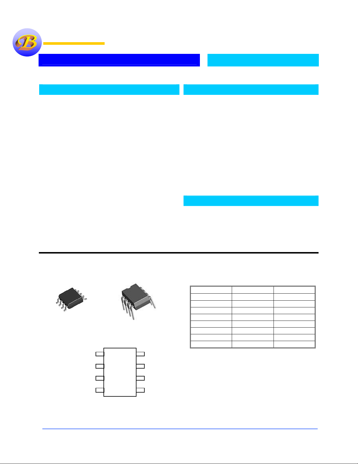
The B39C4X devices are available in 8 pin DIP and SOIC.
Pin Connection
the start-up current is reduced to 50µA (typ.) from
IN
8-SOIC and 8-PDip
COMP
COMP
FB
ISENSE
ISENSE
RT/CT
RT/CT
1
1
2
2
3
3
4
4
8
8
7
7
6
6
5
5
REF
REF
VDD
OUTPUT
OUTPUT
GND
GND
Top
B38C42/43/44/45
Advance Information
Features
• Low-Power BiCMOS Process
• Ultra Low Start-Up Current of 50µA (typ.)
• Very Lower Operating Current (4mA)
• Current Mode Operation ≥ 500KHz
• CMOS outputs with Rail to Rail outputs
• Under Voltage Lockout with Hysteresis
• 5V Trimmed Bandgap Reference
• Trimmed Oscillator Discharged Current
• Low Cross-Conduction Currents
• Available in 8 pin SOIC and 8PDip
• Similar to MIC38C42/43/44/45
• Pin to Pin compatible with UC3842X Family
Applications
• Switched and Current Mode Power Supplies
• Off-line Power Supply
• Step-Up (Buck), Step-Down (Boost) Regulator
• Flyback, Isolated Regulators
• Synchronous FET converters
• Forward Converters
Ordering Information
Devices Package Temp.
B38C42M SO-8
B38C42P 8-DIP
B38C43M SO-8
B38C43P 8-DIP
B38C44M SO-8
B38C44P 8-DIP
B38C45M SO-8
B38C45P 8-DIP
-40°C to +85°C
-40°C to +85°C
-40°C to +85°C
-40°C to +85°C
-40°C to +85°C
-40°C to +85°C
-40°C to +85°C
-40°C to +85°C
Bay Linear, Inc
2418 Armstrong Street, Livermore, CA 94550 Tel: (925) 606-5950, Fax: (925) 940-9556 www.baylinear.com
Page 2
B38C4X
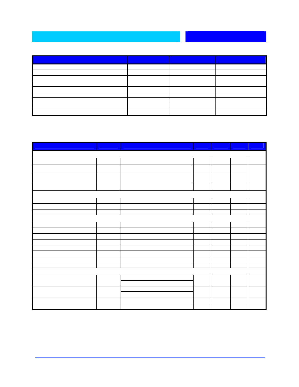
Absolute Maximum Rating
Parameter Symbol Value Unit
Supply Voltage V
Switch Supply Voltage V
Output Current I
DD
D
OUT
Zener Current VDD 30 mA
Current Sense Voltage V
Feedback Voltage V
Power Dissipation P
ISENSE
FB
D
Storage Temperature Range T -65 to 150
Lead Temperature (Soldering 10 Sec.) T
L
20 V
20 V
1A A
-0.3 to 5.5 V
-0.3 to 5.5 V
1 W
°C
300
°C
Electrical Characteristics
VDD = 15V (Note 4), RT = 11k, CT = 3.3nF, TA= -40°C to +85°C, unless otherwise specified
Parameter Symbol Conditions MIN TYP MAX UNIT
REFERENCE SECTION
Reference Voltage V
Line Regulation REG
Load Regulation REG
Short Circuit Output Current I
REF
(LINE)
(LOAD)
SC
OSCILLATOR SECTION
Oscillator Frequency f
Frequency Change with Voltage
Oscillator Amplitude V
∆f/∆V
OSC
ERROR AMPLIFIER SECTION
Input Bias Current I
Input Voltage V
Open Loop Voltage Gain G
BIAS
I(E>A)
VO
Power Supply Rejection Ratio PSRR
Output Sink Current I
Output Source Current I
High Output Voltage V
Low Output Voltage V
SINK
SOURCE
OH
OL
OUTPUT SECTION
Low Output Voltage V
High Output Voltage V
Rise Time t
Fall Time t
OL
OH
R
F
TJ = 25 °C. I
12V≤VDD≤18V, IO = 5µA
1mA≤I
REF
= 1mA
REF
≤20mA
T= 25 °C
T= 25 °C
12V≤VCC≤25V
CC
- 1.6 2.3 V
-1 -0.1 1
V1 =2.5V 2.42 2.50 2.58 V
2V≤VO≤4V
CC
≤25V
12V≤V
V2 =2.7V, V1 =1.1V 2 6 - mA
V2=2.3, V1=5V -0.5 -1.0 - mA
V2=2.3, RL= 15Ω to GND
V2=2.7, RL= 15Ω to pin 8
I
= 20mA
SINK
I
= 200mA
SINK
S
= 20mA
ource
S
= 200mA
ource
TJ = 25 °C, CL=1nF (note3)
TJ = 25 °C, CL=1nF (note3)
4.90 5.00 5.10 V
- 2 20
mV
- 1 25
-30 -80 -180 mA
47 52 57 KHz
- 0.05 1 %
P-P
µA
65 90 - dB
60 70 - dB
5 6 - V
- 0.8 1.1 V
-
13
12
0.08
1.4
13.5
13.0
0.4
2.2
-
-
V
V
- 40 70 ns
- 30 50 ns
Note: Output Switch tests are performed under pulsed conditions to minimize power dissipation
Bay Linear, Inc
2418 Armstrong Street, Livermore, CA 94550 Tel: (925) 606-5950, Fax: (925) 940-9556 www.baylinear.com
Page 3

B38C4X
Electrical Characteristics
(VCC = 15V;RT = 10Ω, CT = 3.3nF, TA=0 °C to +70°C, unless otherwise specified)
Parameter Symbol Conditions MIN TYP MAX UNIT
CURRENT SENSE SECTION
Gain G
Maximum input Signal V
Power Supply Rejection
Ratio
Input Bias Current I
UNDER-VOLTAGE LOCKOUT SECTION
Start Threshold V
Min-Operating Voltage
(after Turn On)
PWM SECTION
Max Duty Cycle D(MAX)
Min Duty Cycle D (MIN) - - 0 %
TOTAL STANDBY CURRENT
Start-Up Current I
Operating Supply Current I
Zener Voltage V
Start-Up Current I
PACKAGE THERMAL RESISTANCE
8-SOIC θ
8-PDip θ
I(MAX) V1
PSRR
BIAS
TH(ST)
V
OPR(MIN)
CC(OPR) V3=V2
(Note 1 & 2) 2.85 3 3.15 V/V
V
ST
Z
ST
JA
JA
= 5V (Note 1) 0.9 1 1.1 V
12V≤V
-3 -10
B3842/B3844 14.5 16 17.5
B3843/B3845 7.8 8.4 9
B3842/B3844 8.5 10 11.5
B3843/B3845 7.0 7.6 8.2
B3842/B3844
B3843/B3845
B3842A/43A/44A/45A - 100 120
B3842B/43B/44B/45B 100 120
I
CC
B3842A/43A/44A/45A - 0.17 0.3 mA
170
≤25V
CC
=ON - 14 17 mA
70 - dB
µA
V
V
95
47
30 38 - V
125
97
48
100
50
%
µA
°C/W
°C/W
14 Pin versions
Bay Linear, Inc
This is
The base
2418 Armstrong Street, Livermore, CA 94550 Tel: (925) 606-5950, Fax: (925) 940-9556 www.baylinear.com
Page 4

B38C4X
Startup & Operating Voltage Selection Guide
Duty Cycle
0% to 96% B38C43 B38C42
0% to 50% B38C45 B38C44
Star-Up at 8.4V
Operating Min= 7.6V
UVLO Thresholds
Star-Up at 14.5V
Operating Min= 9.0V
Pin Descriptions
Pin No.# Name Function
1 COMP Output of error amplifier & input to PWM comparator
2 FB Inverting input of error amplifier
3 ISNS Current sense comparator input. It is internally limited to 1V
4 RT/CT Oscilator RC timing component connection. Resistor RT is connected to
and capacitro CT is conencted to ground. Different values of RT
V
REF
and CT determine the maximum duty cycle..
5 GND/PGND Combined pwoer and analog ground
6 OUT High-power, toten-pole driver output. OUT pin is activly held LOW
is below the UVLO threshold.
CC
7 V
8 V
DD
REF
when V
Suply votlage input
5Volt reerence votlage output
Application Notes:
The Bay Linear B38C4X devices are compatible with
generic 384x PWM devices. The following discussion
highlights the differences and advantages of the Bay C
design.
Start- up Current
Bau Linear BiCMOS process allows for substantial
reduction in the start- up current. Typical start- up
current is 95 µ A, with a maximum limit of 120 µ A.
Low start- up current allows high resistance, lowerwattage, start- up resistors to supply controller start-
up power
.
Output Driver
The B38C4x CMOS output stage drives external
power MOSFETs to the full supply voltage. Low ONresistance and high peak current drive combine to give
greater than 1000pF gate capacitance drive capability.
Rise and fall time requirements may dictate the
appropriate value of output capacitance. Within the
restrictions of output capacity and controller power
dissipation, switching frequencies
can exceed 1MHz.
The CMOS output stage “ break- before- make”
action is guaranteed by design and insures that no
cross- conduction current will flow. This
minimizes heat dissipation, increases efficiency
and enhances reliability.
Oscilator Operation
Two external components, RT and CT, set the
switching frequency.
With VCC = 14V, RT = 10k and CT = 3.3nF,
nominal switching frequency is 50kHz.
B38C4X
Bay Linear, Inc
2418 Armstrong Street, Livermore, CA 94550 Tel: (925) 606-5950, Fax: (925) 940-9556 www.baylinear.com
Page 5

Advance Information- These data sheets contain descriptions of products that are in development. The specifications are based on the engineering calculations,
computer simulations and/ or initial prototype evaluation.
Preliminary Information- These data sheets contain minimum and maximum specifications that are based on the initial device characterizations. These limits are
subject to change upon the completion of the full characterization over the specified temperature and supply voltage ranges.
The application circuit examples are only to explain the representative applications of the devices and are not intended to guarantee any circuit
design or permit any industrial property right to other rights to execute. Bay Linear takes no responsibility for any problems related to any
industrial property right resulting from the use of the contents shown in the data book. Typical parameters can and do vary in different
applications. Customer’s technical experts must validate all operating parameters including “ Typical” for each customer application.
LIFE SUPPORT AND NUCLEAR POLICY
Bay Linear products are not authorized for and should not be used within life support systems which are intended for surgical
implants into the body to support or sustain life, in aircraft, space equipment, submarine, or nuclear facility applications without
the specific written consent of Bay Linear President.
Bay Linear, Inc
2418 Armstrong Street, Livermore, CA 94550 Tel: (925) 606-5950, Fax: (925) 940-9556 www.baylinear.com
 Loading...