

Page 1
Bay Linear, Inc
2418 Armstrong Street, Livermore, CA 94550 Tel: (925) 606-5950, Fax: (925) 940-9556 www.baylinear.com
Current Mode PWM Controller
B3842/43/44/45A&A1
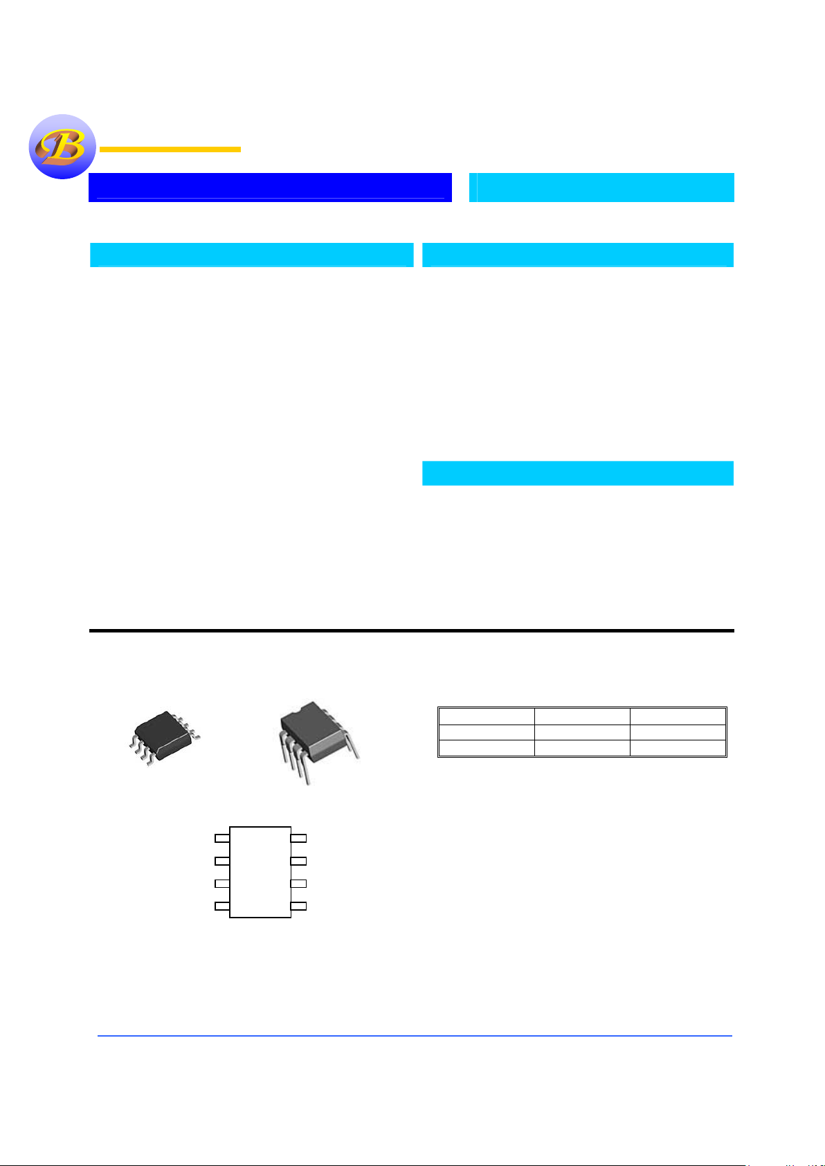
Pin Connection
Ordering Information
Devices Package Temp.
B384X(Z)M SO-8
0 °C to 70 °C
B384X(Z)P 8-DIP
0 °C to 70 °C
Z=A ON Semi Z=A1 Fairchild & Samsung
Description
The Bay Linear B3842/43/44/45 are fixed frequency currentmode PWM controller. These devices are designed for OffLine and DC-to-DC converter applications with minimum
external components. The B3842 family Feature a trimmed
oscillator for precise duty cycle control, a temperature
compensated reference, high gain error amplifier, current
sensing comparator, and a high current totempole output.
Ideally suited for driving a power N-Channel MOSFET’s. It is
low when is on off stage. Protection circuitry includes built in
under-voltage lockout and current limiting.
Major differences between members of these series are the
UVLO thresholds and maximum duty-cycle ranges. Typical
UVLO thresholds of 16V (on) and 10V (off) on the B3842 and
B3844 devices make them ideally suited to off-line
applications. These corresponding typical thresholds for the
B3842 and B3845 devcies are 8.4V (on) and 7.6V (off). The
B3842 and B3843 devcies can operate to duty cycles
approaching 100%. A duty-Cycle range of 0 to 50% is
obtained by the B3844 and B3845 by the addition of an
internal toggle flip-flop, which blanks the output off every
other clock cycle. It id available in 8 pin DIP and SOIC
packages.
Features
• Low Start-Up and Operating Current
• Maximum Duty Cycle
• Operating Frequency Up to 500KHz
• Under voltage Lockout with Hysteresis
• Available in 8 pin SOIC
• Similar to industry Standard UC3842
Applications
• Switching Power Supply
• Monitor
2
1
3
4
8
7
6
5
8-Pin Surface Mount
Top View
COMP
ISENSE
RT/CT
GND
VCC
OUTPUT
REF
NC
2
1
3
4
8
7
6
5
8-Pin Surface Mount
Top View
COMP
ISENSE
RT/CT
GND
VCC
OUTPUT
REF
NC
Bay Linear
Inspire the Linear Power
Page 2
Bay Linear, Inc
2418 Armstrong Street, Livermore, CA 94550 Tel: (925) 606-5950, Fax: (925) 940-9556 www.baylinear.com
B384X
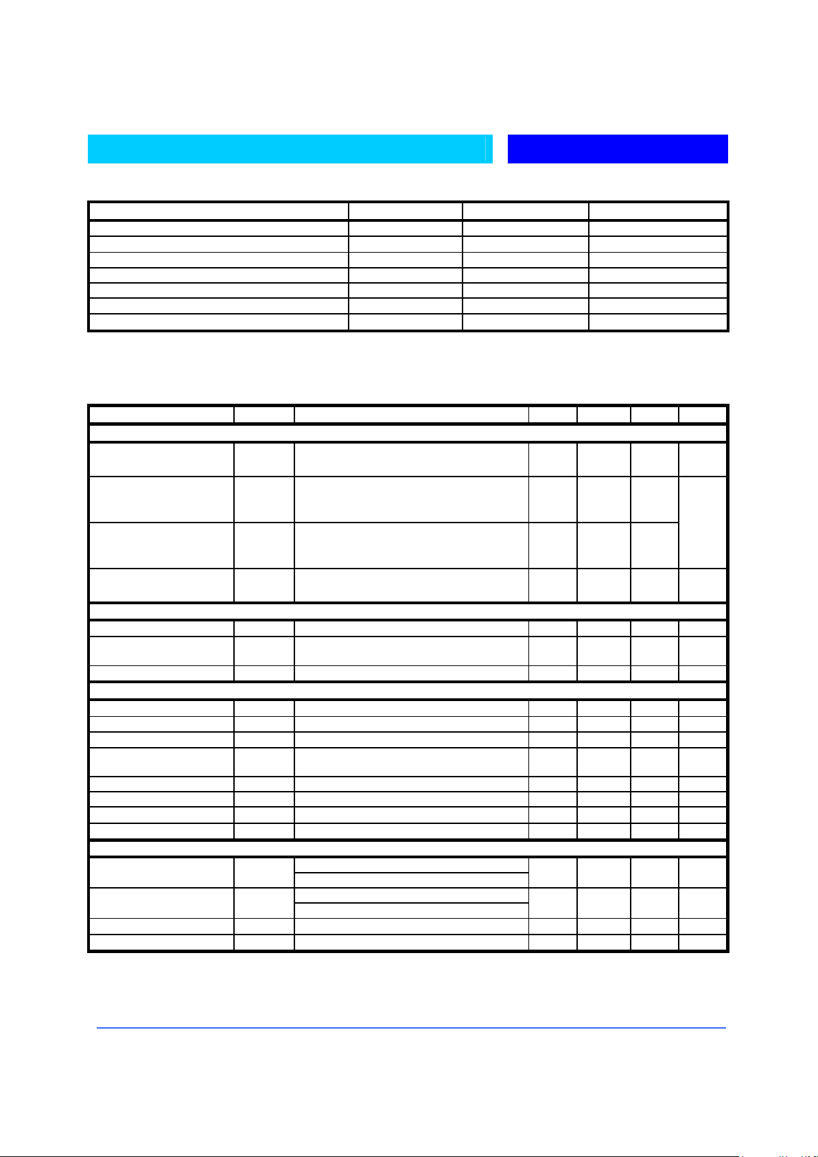
Absolute Maximum Rating
Parameter Symbol Value Unit
Supply Voltage V
CC
30 V
Output Current I
O
±1
A
Analog Input (pin 2,3) V
(ANA)
-0.3 to 6.3 V
Error Amp Output Sink Current I
SINK (E.A)
10 mA
Power Dissipation P
D
1 W
Storage Temperature Range T -65 to 150
°C
Lead Temperature (Soldering 10 Sec.) T
L
260
°C
Electrical Characteristics
(VCC = 15V;RT = 10Ω, CT = 3.3nF, TA=0 °C to +70°C, unless otherwise specified)
Parameter Symbol Conditions MIN TYP MAX UNIT
REFERENCE SECTION
Reference Voltage V
REF
TJ = 25 °C. I
REF
= 1mA
4.90 5.00 5.10 V
Line Regulation REG
(line)
12V≤VCC≤25V
- 6 20
Load Regulation REG
(LOAD)
1mA≤I
REF
≤20mA
T= 25 °C
- 6 25
mA
Short Circuit Output
Current
I
SC
T= 25 °C
- -100 -180 mA
OSCILLATOR SECTION
Oscillator Frequency f
T= 25 °C
47 52 57 KHz
Frequency Change with
Voltage
∆f/∆V
CC
12V≤VCC≤25V
- 0.05 1 %
Oscillator Amplitude V
OSC
- 1.6 - V
P-P
ERROR AMPLIFIER SECTION
Input Bias Current I
BIAS
- -0.1 -2
µA
Input Voltage V
I(E>A)
V1 =2.5V 2.42 2.50 2.58 V
Open Loop Voltage Gain G
VO
2V≤VO≤4V
65 90 - dB
Power Supply Rejection
Ratio
PSRR
12V≤V
CC
≤25V
60 70 - dB
Output Sink Current I
SINK
V2 =2.7V, V1 =1.1V 2 7 - mA
Output Source Current I
SOURCE V2
=2.3, V1=5V -0.6 -1.0 - mA
High Output Voltage V
OH
V2=2.3, RL= 15Ω to GND
5 6 - V
Low Output Voltage V
OL
V2=2.7, RL= 15Ω to pin 8
- 0.8 1.1 V
OUTPUT SECTION
I
SINK
= 20mA Low Output Voltage V
OL
I
SINK
= 200mA
- 0.08
1.4
0.4
2.2
V
S
ource
= 20mA High Output Voltage V
OH
S
ource
= 200mA
13
12
13.5
13.0
-
-
V
Rise Time t
R
TJ = 25 °C, CL=1nF (note3)
- 45 150 ns
Fall Time t
F
TJ = 25 °C, CL=1nF (note3)
- 35 150 ns
Note: Output Switch tests are performed under pulsed conditions to minimize power dissipation
Page 3

Bay Linear, Inc
2418 Armstrong Street, Livermore, CA 94550 Tel: (925) 606-5950, Fax: (925) 940-9556 www.baylinear.com
B384X
Electrical Characteristics
(VCC = 15V;RT = 10Ω, CT = 3.3nF, TA=0 °C to +70°C, unless otherwise specified)
Parameter Symbol Conditions MIN TYP MAX UNIT
CURRENT SENSE SECTION
Gain G
V
(Note 1 & 2) 2.85 3 3.15 V/V
Maximum input Signal V
I(MAX) V1
= 5V (Note 1) 0.9 1 1.1 V
Power Supply Rejection
Ratio
PSRR
12V≤V
CC
≤25V
70 - dB
Input Bias Current I
BIAS
-3 -10
µA
UNDER-VOLTAGE LOCKOUT SECTION
B3842/B3844 14.5 16 17.5
Start Threshold V
TH(ST)
B3843/B3845 7.8 8.4 9
V
B3842/B3844 8.5 10 11.5
Min-Operating Voltage
(after Turn On)
V
OPR(MIN)
B3843/B3845 7.0 7.6 8.2
V
PWM SECTION
B3842/B3843
Max Duty Cycle D(MAX)
B3844/B3845
95
47
97
48
100
50
%
Min Duty Cycle D (MIN) - - 0 %
TOTAL STANDBY CURRENT
B3842A/43A/44A/45A - 0.17 0.3
Start-Up Current I
ST
B3842A1/43A1/44A1/45A1 0.45 1
mA
Operating Supply Current I
CC(OPR) V3=V2
=ON - 14 17 mA
Zener Voltage V
Z
I
CC
30 38 - V
Block Diagram
Page 4

Bay Linear, Inc
2418 Armstrong Street, Livermore, CA 94550 Tel: (925) 606-5950, Fax: (925) 940-9556 www.baylinear.com
B384X
Figure 1: Error Amp Configuration
Figure 2: Under-Voltage Lockout
Figure 3: Current Sense Circuit
3842
3843
Page 5

Bay Linear, Inc
2418 Armstrong Street, Livermore, CA 94550 Tel: (925) 606-5950, Fax: (925) 940-9556 www.baylinear.com
B384X
Page 6

Bay Linear, Inc
2418 Armstrong Street, Livermore, CA 94550 Tel: (925) 606-5950, Fax: (925) 940-9556 www.baylinear.com
B384X
Figure 4: Slope Conpensation Techigues
Figure 5:Latched Shutdown
B3842A
B3842A
Page 7

Bay Linear, Inc
2418 Armstrong Street, Livermore, CA 94550 Tel: (925) 606-5950, Fax: (925) 940-9556 www.baylinear.com
B384X
Page 8

Bay Linear, Inc
2418 Armstrong Street, Livermore, CA 94550 Tel: (925) 606-5950, Fax: (925) 940-9556 www.baylinear.com
B384X
Page 9

Bay Linear, Inc
2418 Armstrong Street, Livermore, CA 94550 Tel: (925) 606-5950, Fax: (925) 940-9556 www.baylinear.com
B384X
Page 10

Bay Linear, Inc
2418 Armstrong Street, Livermore, CA 94550 Tel: (925) 606-5950, Fax: (925) 940-9556 www.baylinear.com
Advance Information- These data sheets contain descriptions of products that are in development. The specifications are based on the engineering calculations,
computer simulations and/ or initial prototype evaluation.
Preliminary Information- These data sheets contain minimum and maximum specifications that are based on the initial device characterizations. These limits are
subject to change upon the completion of the full characterization over the specified temperature and supply voltage ranges.
The application circuit examples are only to explain the representative applications of the devices and are not intended to guarantee any circuit
design or permit any industrial property right to other rights to execute. Bay Linear takes no responsibility for any problems related to any
industrial property right resulting from the use of the contents shown in the data book. Typical parameters can and do vary in different
applications. Customer’s technical experts must validate all operating parameters including “ Typical” for each customer application.
LIFE SUPPORT AND NUCLEAR POLICY
Bay Linear products are not authorized for and should not be used within life support systems which are intended for surgical
implants into the body to support or sustain life, in aircraft, space equipment, submarine, or nuclear facility applications without
the specific written consent of Bay Linear President.
 Loading...