

Page 1
Bay Linear
Inspire the Linear Power
Switching Regulator Controller
Step Up Low Voltage (BIPOLAR)
Description
The Bay Linear B3800 series is monolithic control circuit
containing the primary functions required for DC-to-DC
converters. This device is design for low voltage applications
incorporating a soft start function and sort circuit detection
function. The device has a low minimum operating voltage of
1.8V and is ideal for the power supply of battery-operated
electronic equipments.
This series was specially designed to be incorporated in StepDown and voltage-inverting applications with a minimum
number of external components.
The B3800 is offer in 8-pin DIP or Surface mount package.
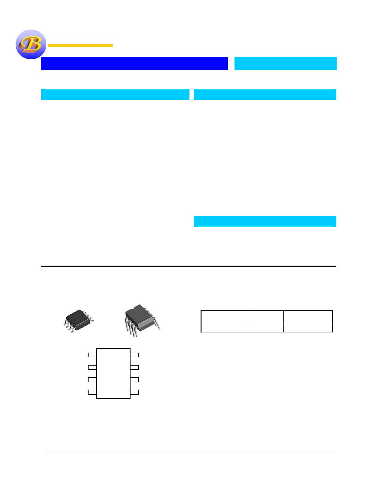
Pin Connection
8-Pin Su rface Mount
8-
8-Pin Su rface Mount
8-
-IN
-IN
SCP 2
SCP 2
1
1
1
1
2
2
8
8
8
8
FB
FB
7
7
7
7
OSC
OSC
BR/CTL
BR/CTL
Vcc
Vcc
3
3
3
3
4
4
4
4
6
6
6
6
GND
GND
5
5
5
5
OUT
OUT
Features
• Wide operation from…………... 1.8 to 15V
• Low Standby Current……………….. 1 µA
• Low Current Consumption……… 5.5mA
• high Speed Operation ……………. 1MHz
Incorporates soft start circuit
•
•
Incorporates a stand-by function
Incorporate a times-latch short circuit
•
detection circuit (SCP)
• Totem-pole type output with adjustable
on/off current (for NPN transistor)
• The error amplifier gain is set inside the
IC, so peripheral components are
minimized.
• Direct Replacement for MB3800
Applications
• Digital Camera
• MP3
• Low Battery Operating Applications
Ordering Information
SO-8
8-pin
B3800M B3800P
P-DIP
8-pin
Operating
Temp. Range
-40°C to 85°C
B3800
Bay Linear, Inc
To p V i e w
To p V i e w
2418 Armstrong Street, Livermore, CA 94550 Tel: (925) 606-5950, Fax: (925) 940-9556 www.baylinear.com
Page 2
B3800
PIN Description
Pin No. Symbol I/O Description
1 -IN I
2 SCP 3 V
CC
4 BR/CTL I
5 V
OUT
6 GND 7 OSC 8 FB O
Error amplifier inverting
Soft start and SCP setting capacitor connection pin
Power supply pin
-
Output current setting and control pin
Totem-pole type output pin
O
Ground pin
Capacitor and resistor connection pin setting the oscillation frequency
Error amplifier output pin
Absolute Maximum Rating
Parameter Symbol Value Unit
Supply Voltage V
Output source current I
Output sink current I
Allowable dissipation
Operating temperature T
Storage temperature Tstg -55 to +125
WARNING: Semiconductor devices can be permanently damaged by application of stress (voltage, current, temperature, etc.) in
excess of absolute maximum ratings. Do not exceed these ratings.
SOP-8, Ta≤+25°C
SOP-8, T
SSOP-8, T
CC
+
O
-
O
≤+25°C
a
≤+25°C 580 mW
a
op
16 V
-50 mA
50 mA
570 mW
430 mW
-30 to +85
°C
°C
Recommended Operating Condition
Parameter Symbol
Power Supply Voltage V
Error amplifier input voltage V
BR/CTL pin input voltage V
Output source current I
Output sink current I
SCP pin capacitance C
Phase compensation capacitance C
Output current setting resistance
Timing resistance
Timing Capacitance C
Oscillation frequency f
Operation temperature
WARNING: Recommended operating conditions are normal operating ranges for the semiconductor device. All the device’s
electrical characteristics are warranted when operated within these ranges. Always use semiconductor devices within the
recommended operating conditions. Operation outside these ranges may adversely affect reliability and could result in device
failure.
No warranty is made with respect to uses, operating conditions, or combinations not represented on the data sheet. Users
considering application outside the listed conditions are advised to contact Bay Linear.
R
R
OSC
T
CC
I
BR
+
O
-
O
PE
P
B
T
T
OP
Min Typ. Max.
1.8 - 15 V
-.0.2 - 1.0 V
-0.2 - V
-40 - - mA
- - 40 mA
- 0.1 - µF
- 0.1 - µF
150 390 5000
1.0 3.0 10.0
100 270 10000 pF
10 500 1000 kHz
-30 +30 +85
Values
CC
Unit
V
Ω
kΩ
°C
Bay Linear, Inc
2418 Armstrong Street, Livermore, CA 94550 Tel: (925) 606-5950, Fax: (925) 940-9556 www.baylinear.com
Page 3

Electrical Characteristics
Parameter Symbol Conditions
Circuit to Prevent
Malfunction at low input
voltage (U.V.L.O.)
Soft Start
(OSC)
Sawtooth wave oscillator
(OSC)
Error amplifier
Idle period adjustable
section
Output section
Output current setting
section/ Control section
Entire device
Reset Voltage V
Threshold voltage
Changing current
Voltage at soft start
completion
Charging current I
Threshold voltage V
Oscillation freq. f
Frequency input
stability
Frequency variation
with temperature
Input threshold
voltage
VTinput stability V
VT variation with
temperature
Input bias current I
Voltage gain
Frequency bandwidth
Maximum output
voltage range
Output source current I
Output sink current I
Maximum duty cycle
Output voltage
Output source current I
Output sink current I
Pull down resistance R
Pin Voltage V
Input off condition I
Input on condition I
Pin current range I
Stand-by current I
Average supply
current
Value
B3800
Unit
Min. Typ. Max.
R
V
TH
I
CS
V
TS
cpc
PC
ocs
f
dv
f
dt
V
T
Tdv
V
TDT
B
A
V
BW A
+
V
OM
-
V
OM
+
OM
_
OM
t
DUTY
V
OH1
V
OH2
V
OL1
V
OL2
+
O
-
O
O
BR
OFF
ON
BR
CCB
I
CC
-
V
=0V 0.7 0.8 0.9 V
SCP
V
=0V -1.5 -1.0 -0.7 µA Short Circuit detection
SCP
- 0.7 0.8 0.9 V
RT=3.0kΩ, CT=270pF
VCC=2V to 15V - 2 10 %
Ta=-30°C to +85°C
VFB=450mV 480 500 520 mV
VCC= 2V to 15V - 5 20 mV
Ta= -30°C to +85°C
VIN=0V -1.0 -0.2 1.0 µA
- 70 100 145
=0dB - 6 -
V
-
VFB=0.45V
RT=3.0kΩ, CT=270pF
V
=0.8V
FB
RB=390Ω, IO= -15mA
RB=750Ω, IO= -10mA,
=1.8V
V
CC
RB=390Ω, IO=15mA
RB=750Ω, IO=10mA,
V
=1.8V
CC
RB=390Ω, VCC=0.9V
RB=390Ω, VCC=0.3V
- 20 30 40
RB=390Ω,
-
BR/CTL pin open or
V
cc
RB=390Ω,
- - 0.9 V
1.1 1.3 1.5 V
-1.5 -1.0 -0.7 µA
400 500 600
kH
z
- 5 - %
- 1 - %
V/
V
M
Hz
0.78 - 0.87
0.05
-
0.2
V
- -40 -24 µA
24 40 - µA
65 75 85 %
1.0 1.2 - V
0.8 1.0 - V
- 0.1 0.2 V
- 0.1 0.2 V
- -30 -20 mA
30 60 - mA
kΩ
0.2 0.3 0.4 V
-20 - 0 µA
- - -45 µA
-1.8 - -0.1 mA
- - 1 mA
- 5.5 9.3 mA
Bay Linear, Inc
2418 Armstrong Street, Livermore, CA 94550 Tel: (925) 606-5950, Fax: (925) 940-9556 www.baylinear.com
Page 4

TIMMING DIAGRAM
BLOCK DIAGRAM
B3800
Bay Linear, Inc
2418 Armstrong Street, Livermore, CA 94550 Tel: (925) 606-5950, Fax: (925) 940-9556 www.baylinear.com
Page 5

Typical Characteristics
B3800
Bay Linear, Inc
2418 Armstrong Street, Livermore, CA 94550 Tel: (925) 606-5950, Fax: (925) 940-9556 www.baylinear.com
Page 6

Typical Characteristics (continued)
B3800
Bay Linear, Inc
2418 Armstrong Street, Livermore, CA 94550 Tel: (925) 606-5950, Fax: (925) 940-9556 www.baylinear.com
Page 7

Typical Characteristics (continued)
B3800
Bay Linear
Bay Linear, Inc
B3800
2418 Armstrong Street, Livermore, CA 94550 Tel: (925) 606-5950, Fax: (925) 940-9556 www.baylinear.com
Page 8

Application Descriptions
Power Supply Control Function
Stand- by mode (supply current 1 mA or less) can be set by
connecting the BR/ CTL pin (pin 4) to VCC or by making the
pin open circuit.
Switching Regulator Function
Reference voltage circuit
The reference voltage circuit generates a temperaturecompensated reference voltage (@1.25V) from voltage
supplied from the power supply pin (pin 3). In addition to
providing the reference voltage for the switching regulator, the
circuit also sets the idle period.
Sawtooth wave oscillator
The sawtooth oscillator generates a sawtooth wave (up to 1
MHz) that is stable with respect to the supply voltage and
temperature. The capacitor and resistor that set the oscillation
frequency are connected to the OSC pin (pin 7).
Error amplifier (Error Amp.)
The error amplifier detects the output voltage of the switching
regulator and outputs the PWM control signal. The voltage
gain is fixed, and connecting a phase compensation capacitor
to the FB pin (pin 8) provides stable phase compensation for
the system.
PWM comparator (PWM Comp.)
The voltage comparator has one inverting and three noninverting inputs. The comparator is a voltage/ pulse width
converter that controls the ON time of the output pulse
depending on the input voltage. The output level is high (H)
when the sawtooth wave is lower than the error amplifier
output voltage, soft start setting voltage, and idle period setting
voltage.
Output circuit
The output circuit has a totem pole type configuration and
can drive an external NPN transistor directly. The value
of the ON/ OFF current can be set by a resistor connected
to the BR/ CTL pin (pin 4).
Other Functions
Soft start and short circuit detection
Soft start operation is set by connecting capacitor CPE to
the SCP pin (pin 2). Soft start prevents a current spike on
start- up.
On completion of soft start operation, the SCP pin (pin 2)
stays low and enters the short circuit detection wait state.
When an output short circuit occurs, the error amplifier
output is fixed at VOM+ and capacitor CPE starts
charging. After charging to approximately 0.8 V, the
output pin (pin 5) is set low and the SCP pin (pin 2) stays
low.
Once the protection circuit operates, the circuit can be
restored by resetting the power supply. (See “n HOW TO
SET THE TIME CONSTANT FOR SOFT START AND
SHORT CIRCUIT DETECTION”.)
Circuit to prevent malfunction at low input voltage
Transients when powering on or instantaneous glitches in
the supply voltage can lead to malfunction of the control
IC and cause system damage or failure. The circuit to
prevent malfunction at low input voltage detects a low
input voltage by comparing the supply voltage to the
internal reference voltage. On detection, the circuit fixes
the output pin to low.
The system recovers when the supply voltage rises back
above the threshold voltage of the malfunction prevention
circuit.
B3800
Bay Linear, Inc
2418 Armstrong Street, Livermore, CA 94550 Tel: (925) 606-5950, Fax: (925) 940-9556 www.baylinear.com
Page 9

HOW TO SET THE TIME CONSTANT FOR SOFT
START AND SHORT CIRCUIT DETECTION
Soft Start
At power on, the capacitor CPE connected to the SCP pin
starts charging. The PWM comparator compares the soft start
setting voltage as a proportion of the voltage at the SCP pin
with the sawtooth waveform. The comparison controls the ON
duty of the OUT pin, causing the soft start operation. On
completion of soft start operation, the voltage at the SCP pin
stays low, the soft start setting voltage stays high, and the
circuit enters the output short circuit detection wait state. Soft
start time (The time until the output ON duty reaches
approximately 50%) tS [s] @ 0.35 ´ CPE [mF]
APPLICATION DIAGRAM
B3800
Short Circuit Protection
If the switching regulator output suddenly drops due to
load effect, the error amplifier output (FB pin) is fixed at
VOM + and capacitor CPE starts charging. When the
voltage at the SCP pin reaches approximately 0.8V, the
output pin is set low and the SCP pin stays low. Once the
protection circuit operates, the circuit can be restored by
resetting the power supply. • Short circuit detection time
[s] @ 0.8 ´ CPE [mF]
T
PE
Bay Linear, Inc
B3800
2418 Armstrong Street, Livermore, CA 94550 Tel: (925) 606-5950, Fax: (925) 940-9556 www.baylinear.com
Page 10

B3800
8 pin SOIC
Pin 1
1.27 (0.50)
BSC
5.0 (0.197)
4.8 (0.188)
0.56 (0.022)
0.49 (0.019)
0.45 (0.018)
0.35 (0.014)
Advance Information- These data sheets contain descriptions of products that are in development. The specifications are based on the engineering calculations,
computer simulations and/ or initial prototype evaluation.
Preliminary Information- These data sheets contain minimum and maximum specifications that are based on the initial device characterizations. These limits are
subject to change upon the completion of the full characterization over the specified temperature and supply voltage ranges.
The application circuit examples are only to explain the representative applications of the devices and are not intended to guarantee any circuit
design or permit any industrial property right to other rights to execute. Bay Linear takes no responsibility for any problems related to any
industrial property right resulting from the use of the contents shown in the data book. Typical parameters can and do vary in different
applications. Customer’s technical experts must validate all operating parameters including “ Typical” for each customer application.
LIFE SUPPORT AND NUCLEAR POLICY
Bay Linear products are not authorized for and should not be used within life support systems which are intended for surgical
implants into the body to support or sustain life, in aircraft, space equipment, submarine, or nuclear facility applications without
the specific written consent of Bay Linear President.
Bay Linear, Inc
2418 Armstrong Street, Livermore, CA 94550 Tel: (925) 606-5950, Fax: (925) 940-9556 www.baylinear.com
4.0 (0.158)
3.8 (0.150)
1.75 (0.069)
1.35 (0.053)
0.78 (0.031)
0.61 (0.024)
0.20 (0.008)
0.10 (0.004)
5.2 (0.205)
4.6 (0.181)
0.37 (0.015)
BSC
0.22 (0.009)
0.19 (0.007)
6.2 (0.244)
5.8 (0.228)
°
45
7
0.77 (0.030)
0.64 (0.025)
°
(4 PLCS)
3°-6
7°(4 PLCS)
°
 Loading...