

Page 1
Bay Linear
Inspire the Linear Power
1.5Amp DC-to-DC Converter Control Circuit
Description
The Bay Linear B34063A series is monolithic control circuit
containing the primary functions required for DC-to-DC
converters. These devices consist of an internal temperature
compensated reference, comparator, controlled, duty cycle
oscillator with an active current limit circuit, driver and high
current output switch.
This series was specially designed to be incorporated in StepDown and Step-Up and voltage-inverting applications with a
minimum number of external component.
The B34063A is offer in 8-pin DIP or Surface mount package.
Features
• Operation from 3.0V to 40V input
•
Low Standby Current
• Current Limiting
• Output Switch Current to 1.5A
Output voltage Adjustable
•
•
Frequency Operation to 100 kHz
Precision 2% Reference
•
•
Step-Up-Step Down or inverting Switching
regulator
• Direct Replacement for MC34063
Applications
• CD ROM
• Mother Board
• SMPS Power Supply
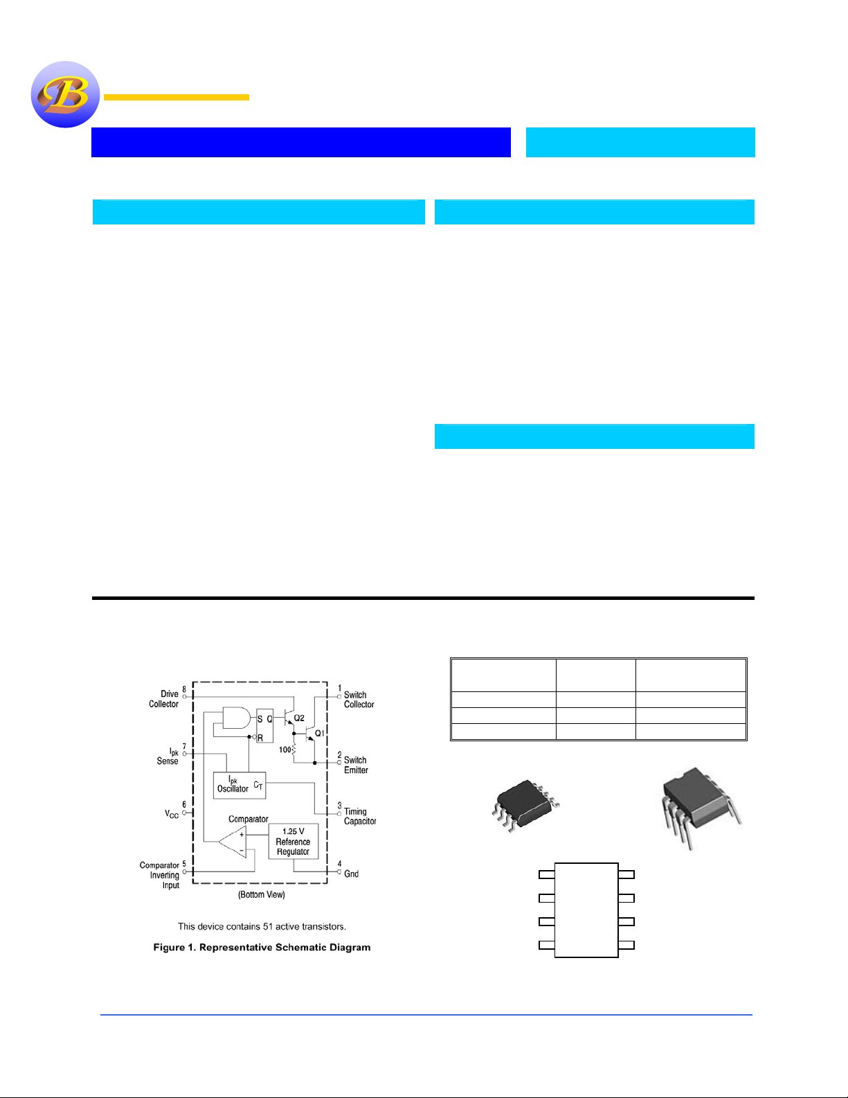
Pin Connection
Ordering Information
SO-8
8-pin
B34063AM B34063AP
B34063AIM B34063AIP
B34063AEM B34063AEP
All Marking will be B34063X. The Temperature will be specified
in out side Box. X=Package type
Switch
Switch
Collector
Collector
Switch
Switch
Emitter
Emitter
Timin g
Timin g
Capacitor
Capacitor
GND
GND
P-DIP
8-pin
8-Pin Surface Mount
8-Pin Surface Mount
1
1
2
2
3
3
4
4
Top View
Top View
8
8
7
7
6
6
5
5
B34063A
Operating
Temp. Range
0°C to 70°C
-40°C to 85°C
-40°C to 125°C
Driver
Driver
Collector
Collector
I
I
Sense
Sense
PK
PK
V
V
CC
CC
Comparator
Comparator
Inverting Input
Inverting Input
Bay Linear, Inc
2418 Armstrong Street, Livermore, CA 94550 Tel: (925) 606-5950, Fax: (925) 940-9556 www.baylinear.com
Page 2
B34063A
Absolute Maximum Rating
Parameter Symbol Value Unit
Supply Voltage V
Comparator Input Voltage Range V
Switch Collector Voltage V
Switch Emitter Voltage V
Switch Collector to Emitter
V
Voltage
Driver Collector Voltage V
Switch Current I
CC
I(COMP)
C(SW)
E(SW)
CE(SW)
C(DR)
SW
40 V
-0.3 ∼ + 40
V
40 V
40 V
40 V
40 V
1.5 I
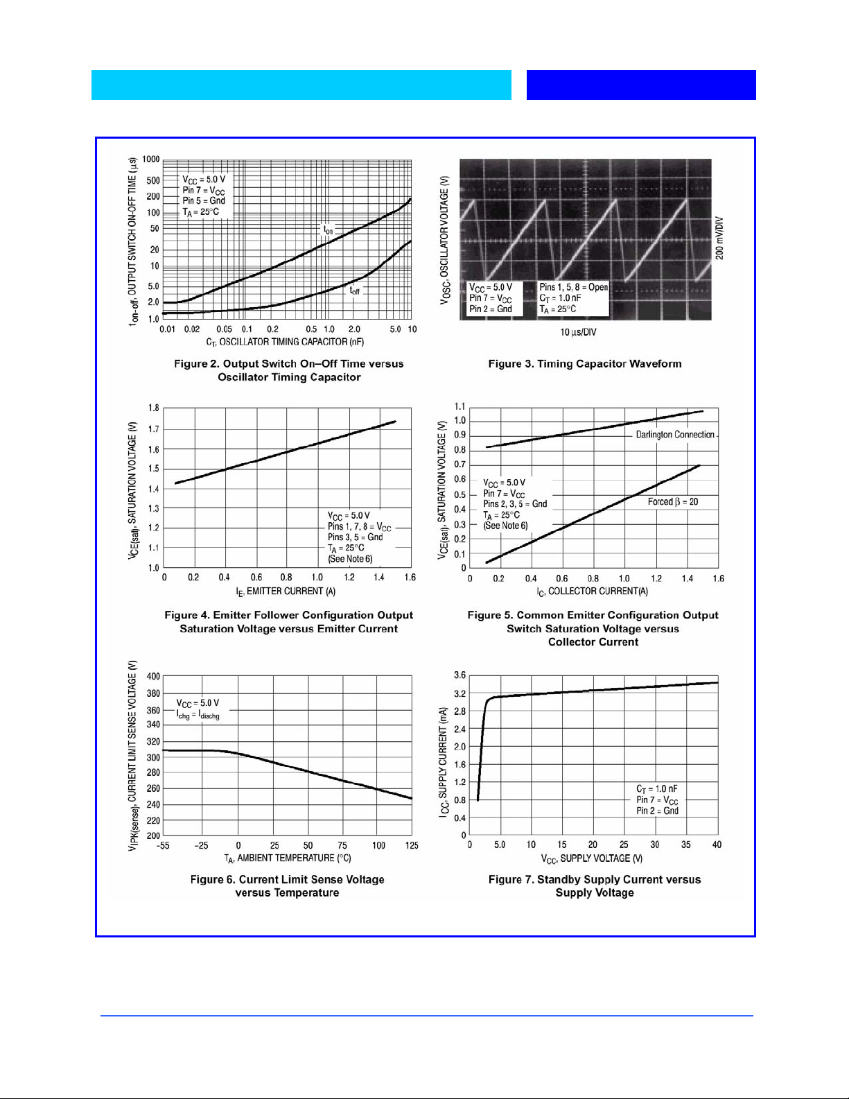
Electrical Characteristics
(V
= 5.0V, TA = T
CC
LOW
to T
(Note 3), unless otherwise specified)
HIGH
Parameter Symbol Conditions MIN TYP MAX UNIT
OSCILATOR
Charging Current I
Discharging Current I
Frequesncy f
Discharge in To Charge
Current Ratio
Current Limit Sense Voltage V
SENSE(C.L)
OUTPUT SWITCH (Note 4)
Saturation Voltage
Darlington Connection
Saturation Voltage (Note 5) V
DC Current Gain G
Collector off Sate Current I
COMPARATOR
Threshold Voltage V
Threshold Voltage Line Reg.
B34063A, B34063AI
B34063AE
Input Bias Current I
TOTAL DEVICE
Supply Current I
V
CE(SAT)
CE(SAT)
∆V
CHG
DISHG
OSC
VVV=5 to 40V, TA = 25 °C
VCC = 5 to 40V, TA = 25 °C
TA = 25 °C
K V7 = V
TA = 25 °C
I
CHG
1
ISW = 1.0A, Pins 1, 8 connected
V
C(drive)
2
I
SW
I(DC)
C(OFF)
TH
BIAS
CC
I
SW
V
CE
TA = 25 °C
T
A
V
TH
CC
VI = 0V -20 -400 nA
VCC = 5V to 40V, CT = 0.001µF,
Pin7=V
Remaining pins open
CC
= I
DISCHG, TA
= V
= 1.0A, V
= 1.0A, V
= 25 °C
C(SW)
= 50mA - 0.45 0.7 V
C(drive)
= 5.0V, TA = 25 °C
CE
= 40V - 40 100
= T
to T
high
LOW
= 3V to 40V
, V5 >V
CC
pin2=Gnd,
TH
24 35 42
140 220 260
µA
µA
24 33 42 kHz
5.2 6.5 7.5 -
250 300 350 mV
- 1.0 1.3 V
50 75 - -
µA
1.225
1.21
-
-
1.25 1.275
1.29
1.4
1.4
5.0
6.0
V
mV
- - 4.0 mA
Note3: T
B34063AE
Note4: Low Duty cycle pulse techniques are used during test to maintain junction temp. as close to ambient temp. as possible.
Note5: If the output switch is driven into hard saturation (non-Darlington configuration) at low switch current (≤300mA) and high driver currents
(≥30mA). It may take up to 2.0 µs for it to come out of saturation. This condition will shorten the off time at frequencies ≥ 30 kHz. And is
magnified at high temperatures. This condition does not occur with a Darlington configuration. Since the output switch can not saturate. If a nonDarlington configuration is used the following output drive condition is recommended:
The 100Ω resistor is the emitter of the driver device requires about 7.0 mA before the output switch conducts
= 0 °C for B34063A, - 40 °C for B34063AI, AE, T
low
Forces β of output switch : Ic output/Ic driver – 7.0mA ≥10
= +70°C for the B34063A, T
high
= +85°C for the B34063AI, +125°C for the
high
Bay Linear, Inc
2418 Armstrong Street, Livermore, CA 94550 Tel: (925) 606-5950, Fax: (925) 940-9556 www.baylinear.com
Page 3
B34063A
Bay Linear, Inc
2418 Armstrong Street, Livermore, CA 94550 Tel: (925) 606-5950, Fax: (925) 940-9556 www.baylinear.com
Page 4

Figure 8. Step-Up Converter
Test Conditions Results
Line Regulation VIN = 8.0 V to 16 V, IO = 175 mA 30 mV = + 0.05%
Load Regulation VIN = 12 V, IO = 75 mA to 175 mA 10 mV = + 0.01%
Output Ripple VIN = 12 V, IO = 175 mA 400 mVp-p
Efficiency VIN = 12 V, IO = 175 mA 89.2%
Output Ripple With Optional Filter VIN = 12 V, IO = 175 mA 40 mVp-p
B34063A
Bay Linear, Inc
2418 Armstrong Street, Livermore, CA 94550 Tel: (925) 606-5950, Fax: (925) 940-9556 www.baylinear.com
Page 5

B34063A
Note 7: If the output switch is driven into hard saturation (non– Darlington configuration) at low switch currents (3 300 mA) and high driver
currents (. 30 mA), it may take up to 2.0 ms to come out of saturation. This condition will shorten the off time at frequencies . 30 kHz, and is
magnified at high temperatures. This condition does not occur with a Darlington configuration, since the output switch cannot saturate. If a non–
Darlington configuration is used, the following output drive condition is recommended.
Bay Linear, Inc
2418 Armstrong Street, Livermore, CA 94550 Tel: (925) 606-5950, Fax: (925) 940-9556 www.baylinear.com
Page 6

Figure 10. Step-Down Converter
Test Conditions Results
Line Regulation VIN = 15 V to 25 V, IO = 500 mA 12 mV = + 0.12%
Load Regulation VIN = 25 V, IO = 50 mA to 500 mA 3.0 mV = + 0.03%
Output Ripple VIN = 25 V, IO = 500 mA 120 mVp-p
Short Circuit Current
Efficiency VIN = 25 V, IO = 500 mA 83.7%
Output Ripple With Optional Filter VIN = 25 V, IO = 500 mA 40 mVp-p
V
= 25 V, RL = 0.1Ω
IN
1.1A
B34063A
Bay Linear, Inc
2418 Armstrong Street, Livermore, CA 94550 Tel: (925) 606-5950, Fax: (925) 940-9556 www.baylinear.com
Page 7

Figure 12. Voltage Inverting Converter
Test Conditions Results
Line Regulation VIN = 4.5 V to 6.0 V, IO = 100 mA 3 mV = + 0.12%
Load Regulation VIN = 5.0 V, IO = 10 mA to 100 mA 0.022 mV = + 0.09%
Output Ripple VIN = 5.0 V, IO = 100 mA 500 mVp-p
Short Circuit Current
Efficiency VIN = 5.0 V, IO = 100 mA 62.2%
Output Ripple With Optional Filter VIN = 5.0 V, IO = 100 mA 70 mVp-p
V
= 5.0 V, RL = 0.1 Ω
IN
910mA
B34063A
Bay Linear, Inc
2418 Armstrong Street, Livermore, CA 94550 Tel: (925) 606-5950, Fax: (925) 940-9556 www.baylinear.com
Page 8

0.56 (0.022)
0.49 (0.019)
Pin 1
1.27 (0.50)
BSC
0.45 (0.018)
0.35 (0.014)
5.0 (0.197)
4.8 (0.188)
4.0 (0.158)
3.8 (0.150)
1.75 (0.069)
1.35 (0.053)
0.78 (0.031)
0.61 (0.024)
0.20 (0.008)
0.10 (0.004)
5.2 (0.205)
4.6 (0.181)
0.37 (0.015)
0.22 (0.009)
0.19 (0.007)
BSC
6.2 (0.244)
5.8 (0.228)
°
45
7
0.77 (0.030)
0.64 (0.025)
°
(4 PLCS)
3°-6
7°(4 PLCS)
B34063A
°
Bay Linear, Inc
2418 Armstrong Street, Livermore, CA 94550 Tel: (925) 606-5950, Fax: (925) 940-9556 www.baylinear.com
Page 9

B34063A
Advance Information- These data sheets contain descriptions of products that are in development. The specifications are based on the engineering calculations,
computer simulations and/ or initial prototype evaluation.
Preliminary Information- These data sheets contain minimum and maximum specifications that are based on the initial device characterizations. These limits are
subject to change upon the completion of the full characterization over the specified temperature and supply voltage ranges.
The application circuit examples are only to explain the representative applications of the devices and are not intended to guarantee any circuit
design or permit any industrial property right to other rights to execute. Bay Linear takes no responsibility for any problems related to any
industrial property right resulting from the use of the contents shown in the data book. Typical parameters can and do vary in different
applications. Customer’s technical experts must validate all operating parameters including “ Typical” for each customer application.
LIFE SUPPORT AND NUCLEAR POLICY
Bay Linear products are not authorized for and should not be used within life support systems which are intended for surgical
implants into the body to support or sustain life, in aircraft, space equipment, submarine, or nuclear facility applications without
the specific written consent of Bay Linear President.
Bay Linear, Inc
2418 Armstrong Street, Livermore, CA 94550 Tel: (925) 606-5950, Fax: (925) 940-9556 www.baylinear.com
 Loading...