

Page 1
Bay Linear
Bay Linear
Bay LinearBay Linear
Inspire the Linear Power
Inspire the Linear Power
Inspire the Linear PowerInspire the Linear Power
Dual USB High Side Power Switch
Description
The Bay Linear B2526 is a dual high-side power switch
recommended for self-powered and bus-powdered universal
serial for bus (USB) application conforming to USB
requirements. USB voltage drop requirements, fault current
limited to 750mA, flag output to indicate fault connections to
the local USB controller are features that meet USB
requirements.
Additional features such as thermal shutdown to prevent
catastrophic switch failure from excessively high current
loads, under voltage lockout (UVLO) to ensure that the device
remains off unless there is a valid input voltage presen t, and
3.3V or 5V logic compatible enable inputs. Two versions of
the enable pin, Active High or Active Low are available in 8pin Dip and 8-pin SOIC packages.
Features
• 3.0V to 5.5V Input
• 110µµµµA Typical on-State Supply Current
• 1µµµµA Typical off-State Supply Current
• 500mA Minimum Continuous Load Current
• 1.25A Maximum Current Limit
• 2.4V Typical Under Voltage Lockout (UVLO)
• Open-Drain Fault Flag Pin
• Thermal Shutdown
• Available with Active-High or Active-Low Enable
Applications
• USB Host and self-Powered Hubs
• USB Power Management
• Battery-Charger Circuits
• Hot Plug-In Power Supplies
• Bus-Powered Hubs
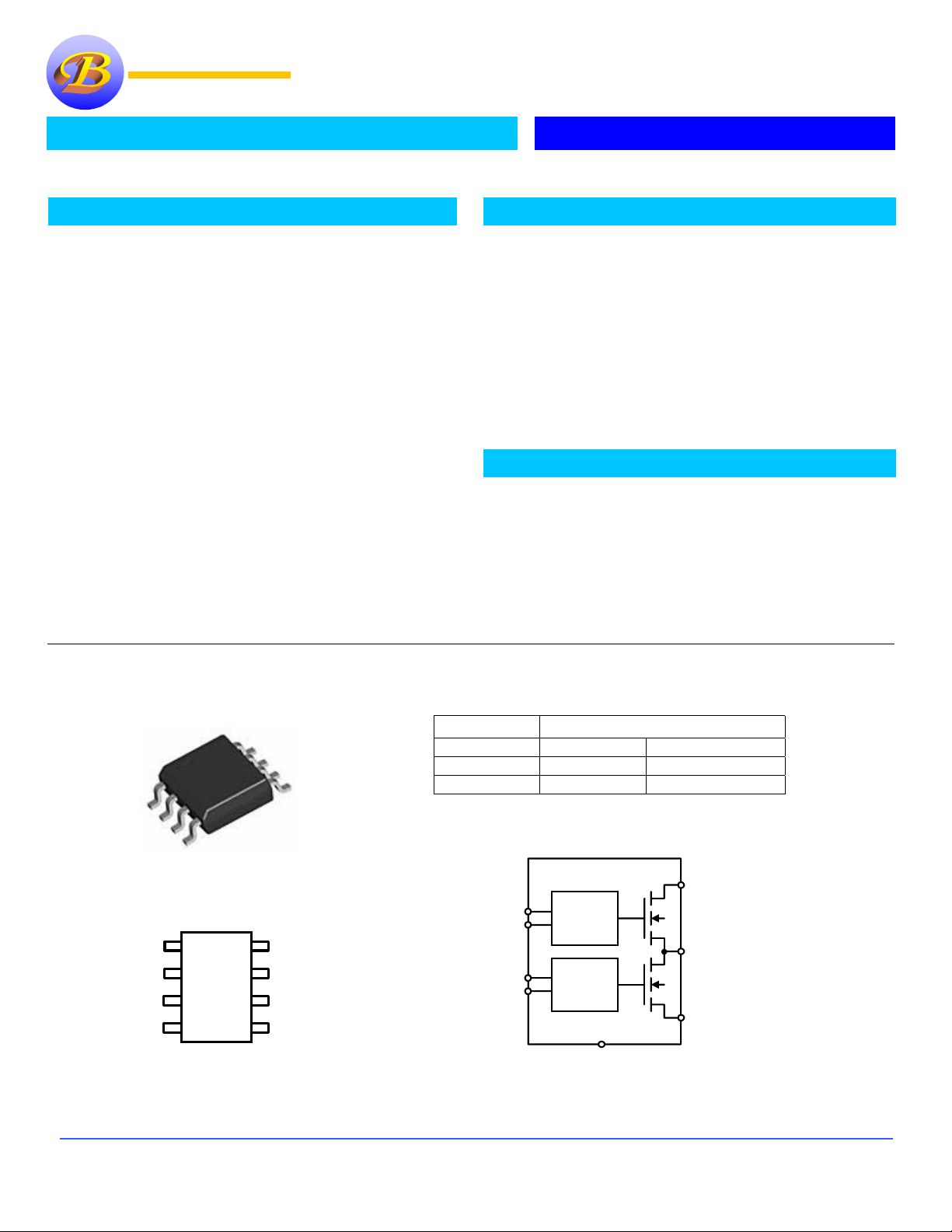
Package Information Ordering Information
Package Enable
Active High Active Low
SO-8 B2526-1M B2526-2M
8 DIP B2526-1P B2526-2P
B2526
EN (A)
FLAG (A)
FLAG (B)
EN (B)
Bay Linear, Inc
8 Out (A)
SO-8
1
2
BAY
B2526
3
4
Top View
EN (A) 1
FLG (A) 2
(A)
V
8
OUT
V
7
IN
6
GND
V
OUT
(B)
5
FLB (B) 3
EN (B) 4
Logic
Charge
Pump
Logic
Charge
Pump
6 GND
7 IN
5 Out (B)
2418Armstrong St., Livermore CA USA 94550 Tel: (925) 606-5950, Fax: (925) 940-9556 www.baylinear.com
Page 2
B2526
ABSOLUTE MAXIMUM RATINGS OPERATING RATING
Supply Voltage…………………………………...6V Supply Voltage..................................................+3V to +5.5V
Fault Flag Voltage………………………………..6V
Ambient Operating Temperature.................... -40°C to +85°C
Fault Flag Current……………………………..50mA
Output Voltage……………………………………6 V
Output Current……………………Internally Limited
Enable Input……………………………-0.3V to 12V
Storage Temperature………………-65°C to +150°C
Lead Temperature (Soldering 5 sec.)………….260°C
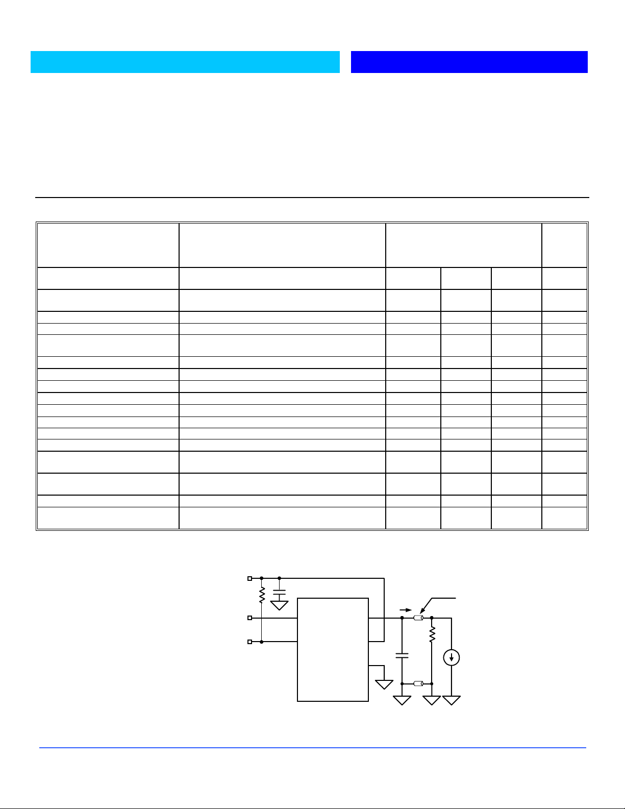
ELECTRICAL CHARACTERISTICS
Parameters
Supply Current (Note1) Switch Off, OUT = Open
Enable Input Threshold Low to High Transition
Enable Input Current VEN = 0V to 5.5V
Enable Input Capacitance 1 pF
Switch Resistance VIN = 5V I
Output Turn-On Delay
Output Turn-On Rise Time
Output Turn-Off Delay
Output Turn-Off Fall Time
Output Leakage Current Each output (output disabled)
Continuous Load Current Each output 0.5 A
Short Circuit Current Limit Each output (enable into load), V
Current Limit Threshold
Over temperature Shutdown
Threshold
Error Flag Output Resistance VIN = 5.0V, IL = 10mA
Error Flag Off Current V
UVLO Threshold VIN = Increasing
General Note: Devices are ESD protected, however, handling precautions recommended.
Note 1: Off is ≤ 0.8V and is ≥ 2.4V for the B2526-1. Off is ≥ 2.4V and on is ≤ 0.8V for the B2526-2. The Enable input has approximately 200mV of hysteresis.
TEST CIRCUIT
(Only 1 Output Shown)
Conditions
(Note1) Switch On, OUT = Open
High to Low Transition, (Note1)
= 3.3V I
V
IN
= 10Ω
R
L
= 10Ω
R
L
= 10Ω
R
L
= 10Ω
R
L
Ramped Load applied to en able output, V
TJ Increasing
TJ Decreasing
= 3.3V, IL = 10mA
V
IN
= 5V
FLAG
= Decreasing
V
IN
OUT
OUT
5V
Thermal Resistance
SOIC..................................................................120°C/W
DIP.....................................................................130°C/W
at V
= 5V, Ta=25°C, unless otherwise specified. (Note 1)
IN
Typ
0.75
110
2.1
1.9
± 0.01 -1 1
= 500mA, Each Switch
= 500mA, Each Switch
OUT
0.1
F
10K
µµµµ
EN (A)
FLG (A)
FLG (B)
EN (B)
= 4.0V 0.5 0.75 1.25 A
≤
4.0V
OUT
B2526
Out (A)
IN
GND
Out (B)
100
140
0.5 ms
1 ms
1 20
1 20
10
1.6 2.2 A
0.01 1
I
OUT
R
C
L
+
L
Ferrite
Bead
Min
0.8
135
125
10
15
2.5
2.3
I
LOAD
(for Current
Limit
Response)
Max
5
160
2.4 V
140
180
V
Units
µ
A
µ
A
mΩ
µ
s
µ
s
µ
A
°
C
Ω
µ
A
Functional Characteristics Test Circuit
Bay Linear, Inc
2418Armstrong St., Livermore CA USA 94550 Tel: (925) 606-5950, Fax: (925) 940-9556 www.baylinear.com
Page 3
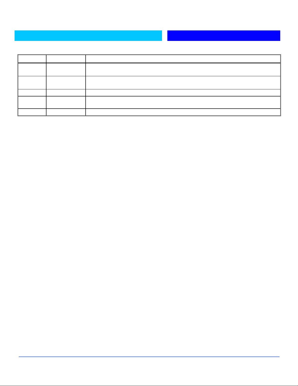
PIN DESCRIPTION
Pin No. Pin Name Pin Function
1 & 4 EN (A)/(B)
2 & 3 FLAG (A)/(B)
6 GND Ground: Supply return.
7 VIN
8 & 5 V
(A)/(B) Switch Output: Output MOSFET source. Typically connect to switched side of load.
OUT
DETAILED DESCRIPITION
Enable (Input): Logic-compatible enables input. High input > 2.1V typical.
Low input < 1.9V typical (B2526-1 active high, B2526 -2 active low).
Fault Flag (Output): Active-low, open-drain output. Indicates over current,
UVLO and thermal shutdown.
Supply Input: Output MOSFET drain. Also supplies IC’s i nternal circuitry. Connect to positive
supply.
B2526
Power Switch
The power switch is an N-Channel MOSFET with a maximum on-state resistance of 140mΩ (V
minimum of 500mA per switch.
Enable
The Logic enable disables the power switch and the bias for the charge pump, driver and other circuitry to reduce the supply current to
less than 5µA when a logic high is present on the EN pin for B2526-2 or a logic low is present on EN for B2526-1. The enable input
is compatible with both TTL and CMOS logic levels.
Driver
The driver controls the gate voltage of the power switch. To Limit large current surges the driver incorporates circuitry that controls
the rise and fall times of the output voltage.
Charge Pump
An internal charge pump supplies power to the driver circuit and provides the necessary voltages to pull the gate of the M OSFET
above the source.
Fault Flag FLG (A)/(B)
FLG is a N-Channel, open drain MOSFET output. The fault flag is active (low) for one or more of the following conditions: undervoltage (while 2V < V
typically 100mV above ground. Multiple FLG pins may be “wired NORed” to a common pull-up resistor.
Thermal Shutdown
An internal thermal sense circuit shuts off the power switch when the junction temperature rises to approximately 150°C. Hysteresis is
built into the thermal sense circuit.
Current Sense
A sense FET monitors the current supplied to the load. When an overload or short circuit is encountered, the current sense circuitry
sends a control signal to the driver. The driver in turn reduces the gate voltage and sends the power FET into its sa turation region,
which switches the output into a constant current mode. The 2526 current-limit profile exhibits a small foldback effect of
approximately 500mA. Once this current-limit threshold is exceeded the device enters constant current mode. The constant current is
specified as the short circuit current limit in the “Electrical Characteristics" table. It is important to note that the 2526 will deliver load
current up to the current-limit Threshold which is typically 1.6A (2.2Amax)."
= 5V). the power switch supplies a
IN
<
2.7V), current limit or thermal shutdown. The flag output MOSFET is capable of sinking a 10mA load to
IN
Under-Voltage Lockout (UVLO)
UVLO prevents the output MOSFET form turning on until V
the switch turns on, if the voltage drops below approximately 2.3V, UVLO shuts off the output MOSFET and signals fault flag.
Under-voltage detection functions only when at least one switch is enabled.
exceeds 2.5V. In the under-voltage state, the FLG will be low. After
IN
Bay Linear, Inc
2418Armstrong St., Livermore CA USA 94550 Tel: (925) 606-5950, Fax: (925) 940-9556 www.baylinear.com
Page 4

B2526
Bay Linear, Inc
2418Armstrong St., Livermore CA USA 94550 Tel: (925) 606-5950, Fax: (925) 940-9556 www.baylinear.com
Page 5

B2526
B4300
B2526
Two-Port Self Powered Hub (Using B2526 & B 43 00)
Bay Linear, Inc
2418Armstrong St., Livermore CA USA 94550 Tel: (925) 606-5950, Fax: (925) 940-9556 www.baylinear.com
Page 6

BLOCK DIAGRAM
B2526
TYPICAL APPLICATION
10K
3.3V USB Controller
V
ON/OFF
IN
Over-Current
µµµµ
0.1
F
Over-Current
ON/OFF
V
5V
0.1
CC
47µ
47µ
47µ47µ
47µ
47µ
47µ47µ
F
µµµµ
F
F
B2526-2
EN (A)
FLG (A)
FLG (B)
EN (B)
100K
100K10K
Out (A)
IN
GND
Out (B)
2 Port USB Self-Powered Hub
Ferrite
Beads
++++
++++
Data
(Two Pair to USB Controller)
V
BUS
D
D
GND
V
BUS
D
D
GND
+
USB
Port
1
+
USB
Port
2
Bay Linear, Inc
2418Armstrong St., Livermore CA USA 94550 Tel: (925) 606-5950, Fax: (925) 940-9556 www.baylinear.com
Page 7

-
Advance Information
or initial prototype evaluation.
These data sheets contain descriptions of products that are in development. The specifications are based on the engineering calculations, computer simulatio ns and/
-
Preliminary Information
completion of the full characterization over the specified temperature and supply voltage ranges.
These data sheets contain minimum and maximum specifications that are based on the initial device characterizations. These limits are subject to change upon the
The application circuit examples are only to explain the representative applications of the devices and are not intended to guarantee any circuit d esign or permit any
industrial property right to other rights to execute. Bay Linear takes no responsibility for any problems related to any industrial property right res ult ing from th e use of
the contents shown i n th e data book. T ypica l pa rameters c an and do va ry in differen t a pplica tions. C ustom er’s tech nic al expert s must vali date a ll opera tin g param eters
including “ Typical” for each customer application.
LIFE SUPPORT AND NUCLEAR POLICY
Bay Linear products are not authorized for and should not be used within life support systems which are intended for surgical implants
into the body to support or sustain life, in aircraft, space equipment, submarine, or nuclear facility applications without the specific
written consent of Bay Linear President.
Bay Linear, Inc
2418Armstrong St., Livermore CA USA 94550 Tel: (925) 606-5950, Fax: (925) 940-9556 www.baylinear.com
 Loading...