

Page 1
Bay Linear, Inc
2418 Armstrong Street, Livermore, CA 94550 Tel: (925) 606-5950, Fax: (925) 940-9556 www.baylinear.com
N-CHANNEL DMOS FET SWITCH
B2520/B2515
VIDEO TRANSISTOR
Series
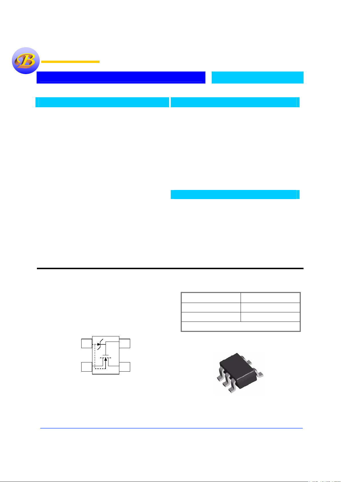
Pin Connection
Ordering Information
Package Part No.
SOT-143 B2520K4 -X.X
SOT-143 B2515K4-XX
Description
The B2520 series consists of enhancement-mode
MOSFETs designed for high speed low-glitch switching
in audio, video, and high-frequency applications. The
B2520 is optimized as a +-7V Switch driver. The B2515
is optimized as an Analog Switch with a 20V Source to
Body breakdown and low Drain Leakage.
The B2500 series uses Bay Linear ULTRA REL DMOS
Process for reliability and robust performance.
These MOSFETs utilize lateral construction to achieve
low capacitance and ultra-fast switching speeds. An
integrated Zener diode provides ESD protection.
Features
• High Input to Output Isolation – 120dB typical
• Low feed through and feedback transients
• Low Inter-electrode Capacitances
• 25V Drain-to Source breakdown for B2520
Application
• High Frequency Drivers
• Video Switches
• A to D Converters
Bay Linear
Inspire the Linear Power
2
14
3
2
14
32
14
3
SOT-143 Package
Lead Code Identification
(top view)
Body
Substrate
Source
Gate
Drain
Page 2

Bay Linear, Inc
2418 Armstrong Street, Livermore, CA 94550 Tel: (925) 606-5950, Fax: (925) 940-9556 www.baylinear.com
B2520/B2515
Electrical Specifications (TC= +25°C unless otherwise noted)
Ohm70507050VGS=5VID=1 mA
V
SB
= 0V
r
DS (ON)
Drain-Source
ON Resistance
V2.01.00.12.01.00.5V
DS=VGSID
=1 µA
V
SB
=0
V
GS (th)
Gate Threshold
Voltage
STATIC
V
DB/SB
= 0
V
GD/BS
=-5
V
GS/BS
=-5 nA501VDS=10V
Gate Leakage
Source - Drain
Leakage
Drain-Source
Leakage
Source-Substrate
Breakdown
Voltage
Drain-Substrate
Breakdown
Voltage
Source-Drain
Breakdown
Voltage
Drain-Source
Breakdown
Voltage
UnitsB2515B2520
Ohm45304530V
GS
=10V
µA101101V
GS
=20VI
GBS
nA501VDS=20V
nA501V
DS
=10VI
S (OFF)
nA501VDS=20V
I
D (OFF)
V2015ID=10 µA, VGB=0
Drain Open
BV
SB
V2015ID=50 nA, VGB=0
Source Open
BV
DB
V152510IS=50 nA
V
GD=VBD
=-5
BV
SD
V
2520
30
25
25
10
ID=10 µA
V
GS=VBS
=0
I
D
=50 nA
V
GS=VBS
=0
BV
DS
BV
DS
MaxTypMinMaxTypMin
Test ConditionsSymbolParameter
Page 3

Bay Linear, Inc
2418 Armstrong Street, Livermore, CA 94550 Tel: (925) 606-5950, Fax: (925) 940-9556 www.baylinear.com
B2520
B2520 B2515 Parameter Symbol Test
Conditions
Min Typ Max Min Typ Max
Units
Common-Source
Forward
Transconductance
gfS
VDS= 10V
ID= 20mA
f = 1MHz,
VSB=0
Pulsed
10 15 10 15 V
Gate Node
Capacitance
C(gs+gd+gb) 2.4 3.5 2.4 3.5 pF
Drain Node
Capacitance
C(gd+db) 1.3 1.5 1.3 1.5 pF
Source Node
Capacitance
C(gs+sb) 3.5 4.0 3.5 4.0 pF
Reverse Transfer
Capacitance
C(dg)
VDS= 10V
VGS=VBS=
-15V
f = 1MHz
0.3 0.5 0.3 0.5 pF
Turn On Delay
Time
td(on) 0.7 1.0 0.7 1.0 ns
Rise Time tr 0.8 1.0 0.8 1.0 ns
DYNAMIC
Turn Off Delay
Time
Td(off)
V∞= 10V
VG(on)=
10V
RL= 680 Ω
RG= 51Ω
CL = 1.5pF
1.5 1.5 ns
Page 4

Bay Linear, Inc
2418 Armstrong Street, Livermore, CA 94550 Tel: (925) 606-5950, Fax: (925) 940-9556 www.baylinear.com
B2520
510 Ω
V
IN
R
L
51 Ω
V
OUT
+V
DD
To
Scope
To
Scope
510 Ω
V
IN
R
L
51 Ω
V
OUT
+V
DD
To
Scope
To
Scope
Input Pulse: t
d
, tr< 1ns
Pulse width: 100 ns
Rep rate: 1 MHz
Sampling Scope
T
r
< 360 ps
R
IN
= 1 MΩ
C
IN
= 2 pF
BW = 500 MHz
Switching Time Test Circuit
+5 V
V
IN
0 V
0 V
V
OUT
V
DD
50%
50%
10%
90%
t
d(on)
t
d(off)
t
f
t
f
Page 5

Bay Linear, Inc
2418 Armstrong Street, Livermore, CA 94550 Tel: (925) 606-5950, Fax: (925) 940-9556 www.baylinear.com
B2520
Advance Information- These data sheets contain descriptions of products that are in development. The specifications are based on the engineering calculations,
computer simulations and/ or initial prototype evaluation.
Preliminary Information- These data sheets contain minimum and maximum specifications that are based on the initial device characterizations. These limits are
subject to change upon the completion of the full characterization over the specified temperature and supply voltage ranges.
The application circuit examples are only to explain the representative applications of the devices and are not intended to guarantee any circuit
design or permit any industrial property right to other rights to execute. Bay Linear takes no responsibility for any problems related to any
industrial property right resulting from the use of the contents shown in the data book. Typical parameters can and do vary in different
applications. Customer’s technical experts must validate all operating parameters including “ Typical” for each customer application.
LIFE SUPPORT AND NUCLEAR POLICY
Bay Linear products are not authorized for and should not be used within life support systems which are intended for surgical
implants into the body to support or sustain life, in aircraft, space equipment, submarine, or nuclear facility applications without
the specific written consent of Bay Linear President.
Absolute Maximum Ratings, Tc= +25°C
Notes:
1. Operation in excess of any one of these conditions may result in
permanent damage to the device
2. T
C
= +25°C, where TCis defined to be the temperature at the
package pins where contact is made to the circuit board.
ESD WARNING: Handling Precautions Should Be Taken To Avoid Static Discharge.
300mWPower dissipation Tc=25
3mW/CLinear Derating Factor
-25 / +20VGate-Drain Voltage
50mAContinuous Drain Current
+30 / +20VDrain-Source Voltage
-15 / +20VGate-Source Voltage
-55 to +125°CStorage Temperature
-55 to +125°CJunction Temperature
SOT-143
Absolute Maximum
[1]
UnitParameter
300mWPower dissipation Tc=25
3mW/CLinear Derating Factor
-25 / +20VGate-Drain Voltage
50mAContinuous Drain Current
+30 / +20VDrain-Source Voltage
-15 / +20VGate-Source Voltage
-55 to +125°CStorage Temperature
-55 to +125°CJunction Temperature
SOT-143
Absolute Maximum
[1]
UnitParameter
 Loading...