

Bay Linear, Inc
2478 Armstrong Street, Livermore, CA 94550 Tel: (925) 606-5950, Fax: (925) 940-9556 www.baylinear.com
5.0A Low Dropout Voltage Regulator
B1585
Adjustable & Fix Output
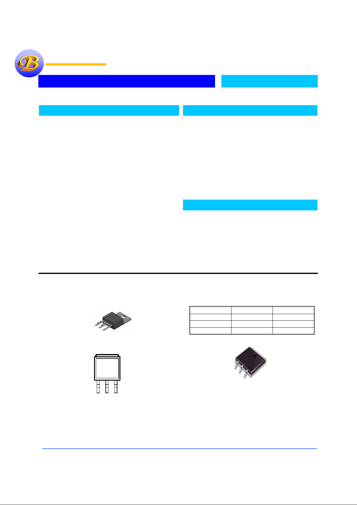
Pin Connection
Ordering Information
Devices Package Temp.
B1585T TO-220
0 °C to 70 °C
B1585S TO-263
0 °C to 70 °C
B1585j LPDD
0 °C to 70 °C
PLDD (J)
Description
The Bay Linear B1585 is Monolithic low power 5.0A
Adjustable and fixed NPN voltage regulator that are easy to
use with minimum external components. It is suitable for
applications requiring a well-regulated positive output voltage
with low input-output differential voltage requirements and
output voltage 1.5V, 2.5V, 3.0V, 3.3V, or 5V.
The B1585 Outstanding features include full power usage up
to 5.0Amp of load current internal current limiting and thermal
shutdown. Other fixed versions are also available consult with
factory.
The B1585 is offered in 3-pin TO-220, LPDD & TO-263
packages compatible with other 3 terminal regulators. For 7A
Low dropout Regulator refer to the B1584 data sheet.
Features
• Adjustable Output Down to 1.2V
• Fixed Output Voltages 2.5V, 3.0V 3.3V,
and 5.0V
• Output Current of 5.0A
• Low Dropout Voltage 1.1V Typ.
• Current & Thermal Limiting
• Standard 3-Terminal Low Cost TO-220,
LPDD, & D
2
Packages
•
Similar to industry Standard
LT1084/LT1585
Applications
• 3.3V to 2.5V for Pentium Processor
• SMPS Post Regulator
• High Efficiency “Green” Computer
Systems
• High Efficiency Linear Power Supplies
• 5V to 3.XXV fro Pentium Processor
• Battery Charger
Top View
TO - 263 - 3 (S)
1
Bay Linear
2
3
Top View
TO - 263 -
1
Bay Linear
2
3
Bay Linear
Bay LinearBay Linear
Bay Linear
Inspire the Linear Power
Inspire the Linear PowerInspire the Linear Power
Inspire the Linear Power
Bay Linear, Inc
2478 Armstrong Street, Livermore, CA 94550 Tel: (925) 606-5950, Fax: (925) 940-9556 www.baylinear.com
B1585
Absolute Maximum Rating
Parameter Symbol Value Unit
Maximum Input Voltage V
IN
7 V
Power Dissipation P
O
Internally Limited W
Thermal Resistance Junction to Case
θ
JC
3
Thermal Resistance Junction to
Ambient
θ
JA
50
°
C/W
Operating Junction
Temperature Range
Control Section
Power Transistor
T
J
0 to 125
0 to 150
Storage Temperature Range T
STG
-65 to 150
Lead Temperature (Soldering 10
Sec.)
T
LEAD
260
°
C
Electrical Characteristics
(VIN = 4.75V to 5.25V; IO = 10mA to 5.0Amp, unless otherwise specified)
Parameter Symbol Conditions MIN TYP MAX UNIT
1.485 1.515
0<I
OUT
<5A, 3.3V<VIN<7V, T= 25 °C
0<I
OUT
<5A, 3.3V<VIN<7V, Over Temp.
1.475
1.5
1.525
2.475 2.525
0<I
OUT
<5A, 4.0V<VIN<7V, T= 25 °C
0<I
OUT
<5A, 4.0V<VIN<7V, Over Temp.
2.460
2.5
2.540
2.970 3.030
0<I
OUT
<5A, 4.5V<VIN<7V, T= 25 °C
0<I
OUT
<5A, 4.5V<VIN<7V, Over Temp.
2.950
3.0
3.050
3.267 3.333
0<I
OUT
<5A, 4.8V<VIN<7V, T= 25 °C
0<I
OUT
<5A, 4.8V<VIN<7V, Over Temp.
3.247
3.3
3.353
4.950 5.050
Output Voltage V
O
0<I
OUT
<5A, 6.5V<VIN<7V, T= 25 °C
0<I
OUT
<5A, 6.5V<VIN<7V, Over Temp.
4.920
5.0
5.080
V
1.238 1.262 Reference Voltage V
ref
VIN<7V, 1.5V<VIN<5.75, 10mA<I
out
<5Amp
1.230
1.250
1.270
V
Line Regulation (1) REG
(line)
IO = 10mA, VIN =5V, T= 25 °C
0.04 0.2
0.08 0.40 Load Regulation (1) REG
(LOAD)
IO = 10mA, VIN =5V, T= 25 °C
%
1.0 Dropout Voltage V
D
T= 25 °C
Over Temperature
1.1 1.3
V
Minimum load Cu rrent I
min
5.0 10 mA
Current Limit I
S
(Vin-V
out
)=3V 5.5 6.8 A
Ground Pin Current I
Q
VIN =5V 6 10 mA
Temperature Stability T
S
IO = 10mA, VIN =5V 0.5 %
Thermal Regulation
T= 25 °C, 30ms pulse
0.003 %/W
Ripple Rejection R
A
T= 25 °C, VIN =5V
60 80 dB
Thermal Resistance - TO-220 Junction to Tab
Junction to Ambient
DD Package Junction to Tab
Junction to Ambient
3.0
60
3.0
60
3.0
60
3.0
60
°
C/W
Note:
Output Switch tests are performed under pulsed conditions to minimize power dissipation

Bay Linear, Inc
2478 Armstrong Street, Livermore, CA 94550 Tel: (925) 606-5950, Fax: (925) 940-9556 www.baylinear.com
B1585
APPLICATION HINTS
The Bay Linear B1585 incorporates protection against
over-current faults, reversed load insertion, over
temperature operation, and positive and nega t ive
transient voltage. However, the use of an output
capacitor is required in order to insure the stability and
the performances.
Stability
The output capacitor is part of the regulator’s
frequency compensation system. Either a 220µF
aluminum electrolytic capacitor or a 47µF solid
tantalum capacitor between the output terminal and
ground guarantees stable operation for all operating
conditions.
However, in order to minimize overshoot and
undershoot, and therefore optimize the design, please
refer to the section ‘Ripple Rejection’.
Ripple Rejection
Ripple rejection can be improved by adding a
capacitor between the ADJ pin and ground. When
ADJ pin bypassing is used, the value of the output
capacitor required increases to its maximum (220µF
for an aluminum electrolytic capacitor, or 47µF for a
solid tantalum capacitor). If the ADJ pin is not
bypass, the value of the output capacitor can be
lowered to 100µF for an electrolytic aluminum
capacitor or 15µF for a solid tantalum capacitor.
However the value of the ADJ-bypass capacitor
should be chosen with respect to the following
equation:
C = 1 / ( 6.28 * F
R
* R1 )
Where C = value of the capacitor in Farads (select
an equal or larger standard value),
F
R
= ripple frequency in Hz,
R
1
= value of resistor R1 in Ohms.
If an ADJ-bypass capacitor is use, the amplitude of the
output ripple will be independent of the output
voltage. If an ADJ-bypass capacitor is not used, the
output ripple will be proportional to the ratio of the
output voltage to the reference voltage:
M = V
OUT
/ V
REF
Where M = multiplier for the ripple seen when the
ADJ pin is optimally bypassed.
V
REF
= Reference Voltage
Reducing parasitic resistance and inductance
One solution to minimize parasitic resistance and
inductance is to connect in parallel capacitors. This
arrangement will improve the transient response of
the power supply if your system requires rapidly
changing current load condition.
Thermal Consideration
Although the B1585 offers some limiting circuitry
for overload conditions, it is necessary not to exceed
the maximum junction temperature, and therefore to
be careful about thermal resistance. The heat flow
will follow the lowest resistance path, which is the
Junction-to-case thermal resistance. In order to
insure the best thermal flow of the component, a
proper mounting is required. Note that the case of
the device is electrically connected to the output. In
case the case has to be electrically isolated, a
thermally conductive spacer can be used. However
do not forget to consider its contribution to thermal
resistance.
Assuming:
V
IN
= 7V, V
OUT
= 5V, I
OUT
= 5A, TA = 90°C,
θ
CASE
=
1°C/W (no external heat sink, no wind)
Power dissipation under these conditions
P
D
= (VIN – V
OUT
) * I
OUT
= 15W
Junction Temperature
T
J
= TA + PD * (
θ
CASE
+
θ
JC
)
For the Control Section
T
J
= 90°C + 15W*(1°C/W + 0.6°C/W) = 114°C
114°C < T
JUNCTION MAX
for the control section.
For the Power Section
T
J
= 90°C + 15W*(1°C/W + 1.6°C/W) = 129°C
129°C < T
JUNCTION MAX
for the power transistor.
In both case reliable operation is insured by
adequate junction temperature.

Bay Linear, Inc
2478 Armstrong Street, Livermore, CA 94550 Tel: (925) 606-5950, Fax: (925) 940-9556 www.baylinear.com
B1585
Basic Adjustable Regulator
Output Voltage
Output Voltage
Consider Figure 2. The resistance R1 generates a constant current flow, normally the specified load current of
10mA. This current will go through the re sistance R
2
to set the overall output voltage. The current I
ADJ
is very
small and constant. Therefore its contribution to the overall output voltage is very small and can generally be
ignored
Load Regulation
Parasitic line resistance can degrade load regulation. In order not to affect the behavior of the regulator, it is best to
connect directly the R
1
resistance from the resistor divider to the case,
and not to the load. For the same reason, it is best to connect the resistor R
2
to the Negative side of the load.
BAY
B1585
Fig.2 Basic Adjustable Regulator
V
OU
T
V
OU
T
V
REF
R
1
R
2
V
OUT
= V
REF
* ( 1 + R2/R1) + I
ADJ
* R
2
I
ADJ
50µA
BAY
B1585
Fig.3 Basic Adjustable Regulator
V
OUT
R
2
R
1
Connect R2 to Load
R
L
Connect R1 to
Case of Regulator
R
P
Parasitic Line
Resistance

Bay Linear, Inc
2478 Armstrong Street, Livermore, CA 94550 Tel: (925) 606-5950, Fax: (925) 940-9556 www.baylinear.com
B1585
Application Diagrams
IN
OUT
ADJ
BAY
B1585
C
1
R
1
R
2
V
OUT
Fig 5. Typical Adjustable Regulator
V
IN
C
2
V
OUT
= V
REF
(1 + R2) + I
ADJ R2
R1
LOAD
ADJ
BAY
B1585
Fig.4 5A Current Output Regulator
V
IN
C
1
R
1
OUT
IN
BAY
B1585
Fig. 6 Improving Ripple Rejection
V
IN
R
1
R
2
150µF
10µF*
121Ω
1%
365Ω
1%
+
+
10µF
C1
*C1 improves ripple rejection. X
C
should be ~ R1 at ripple frequency.
5V
ADJ
IN OUT
(Note A)
Note A: V
IN (MIN)
= ( Intended V
OUT
) + ( V
DROPOUT (MAX)
)
V
OUT
BAY
B1585
Fig.7 5V Regulator with Shutdown
V
IN
100µF
121Ω
1%
365Ω
1%
+
+
10µF
5V
ADJ
IN OUT
(Note A)
Note A: V
IN (MIN)
= ( Intended V
OUT
) + ( V
DROPOUT (MAX)
)
1k
1k
TTL
Output
2N3904

Bay Linear, Inc
2478 Armstrong Street, Livermore, CA 94550 Tel: (925) 606-5950, Fax: (925) 940-9556 www.baylinear.com
B1585
Typical Characteristics

Bay Linear, Inc
2478 Armstrong Street, Livermore, CA 94550 Tel: (925) 606-5950, Fax: (925) 940-9556 www.baylinear.com
B1585
0.103 BSC
0.050 (1.270)
0.600
+
-
0.025
0.405
0.005
0.055 (1.397)
(10.287 0.127)
±
±
0.356 0.005
(9.042 0.127)
±
±
(15.24
0.635)
±
(2.616)
0.032
+
-
0.001
(0.813 0.025)
+
-
0.176
0.005
0.050
0.002
0.015
+
-
0.003
0°
8°
(0.381 0.074)
+
-
0.100 0.010
(2.540
0.254)
±
±
(4.470
0.127)
±
(1.270
0.051)
±
±
±
0.408 ± 0.013
(10.36 ± 0.33)
0.110 ± 0.010
(2.794 ± 0.254)
0.250 ± 0.010
(6.350 ± 0.254)
0.151D ± 0.002
(3.835 D ± 0.051)
0.180 ± 0.005
(4.572 ± 0.127)
0.050 ± 0.002
(1.270 ± 0.051)
0.340 ± 0.010
(8.636 ± 0.254)
0.150 MIN
(3.81 MIN)
0.410
(10.41)
0.100 ± 0.010
(2.540 ± 0.254)
0.032 ± 0.005
(0.813 ± 0.127)
0.540 ± 0.015
(13.720 ± 0.381)
0.050 TYP
(1.27 TYP)
0.200 ± 0.010
(5.080 ± 0.254)
0.015 ± 0.010/-0.002
(0.381± 0.254/-0.051)
0.015 ± 0.010/-0.015
(2.667± 0.254/-0.381)
1.020 ± 0.015
(25.910 ± 0.381)
SEATING PLANE
Tapered 1
o
2 Sides
7o Typ.

Bay Linear, Inc
2478 Armstrong Street, Livermore, CA 94550 Tel: (925) 606-5950, Fax: (925) 940-9556 www.baylinear.com
Advance Information
-
These data sheets contain descriptions of products that are in development. The specifications are based on the engineering calculations,
computer simulations and/ or initial prototype evaluation.
Preliminary Information
-
These data sheets contain minimum and maximum specifications that are based on the initial device characterizations. These limits are
subject to change upon the completion of the full characterization over the specified temperature and supply voltage ranges.
The application circuit exa mples are only to exp lain the representative applications of the devices and are not intended to gu arantee any circuit
design or permit an y in dustrial property righ t to other rights to execute. Bay Linear takes no responsibility for any problems related to any
industrial property right resulting from the use of the contents shown in the data book. Typical parameters can and do vary in different
applications. Customer’s technical experts must validate all operating parameters including “ Typical” for each customer application.
LIFE SUPPORT AND NUCLEAR POLICY
Bay Linear products are not authorized for and should not be used within life support systems which are intended for surgical
implants into the body to support or sustain life, in aircraft, space equipment, submarine, or nuclear facility application s without
the specific written consent of Bay Linear President.
 Loading...