

Page 1
Bay Linear, Inc
2478 Armstrong Street, Livermore, CA 94550 Tel: (925) 606-5950, Fax: (925) 940-9556 www.baylinear.com
5.0A Low Dropout Voltage Regulator
B1581
Adjustable & Fix Output
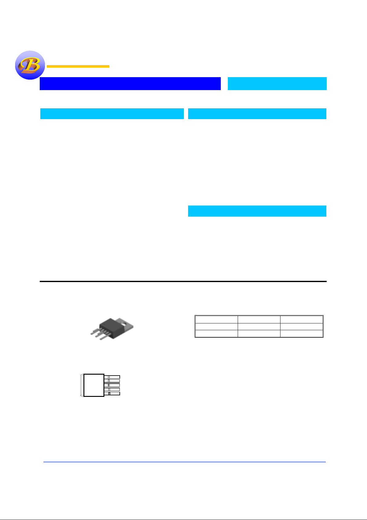
Pin Connection
Ordering Information
Devices Package Temp.
B1581T TO-220
0 °C to 70 °C
B1581S TO-263
0 °C to 70 °C
Description
The Bay Linear B1581 is Monolithic low power 5.0A
Adjustable and fixed NPN voltage regulator that are easy to
use with minimum external components. It is suitable for
applications requiring a well-regulated positive output voltage
with low input-output differential voltage requirements and
output voltage 1.5V, 2.5V, 3.0V, 3.3V, or 5V.
The B1581 Outstanding features include full power usage up
to 5.0Amp of load current internal current limiting and thermal
shutdown. Other fixed versions are also available consult with
factory.
The B1581 is offered in a 5-pin TO-220, & TO-263 packages
compatible with other 5 terminal regulators. For 5A Low
dropout Regulator refer to the B1581 data sheet.
Features
• Adjustable Output Down to 1.2V
• Fixed Output Voltages 2.5V, 3.0V 3.3V,
and 5.0V
• Output Current of 5.0A
• Low Dropout Voltage 700mV Typ.
• Current & Thermal Limiting
• Standard 3-Terminal Low Cost TO-220,
D
2
Packages
•
Similar to industry Standard
EZ1581/CS5205
Applications
• 3.3V to 2.5V for Pentium Processor
• SMPS Post Regulator
• High Efficiency “Green” Computer
Systems
• High Efficiency Linear Power Supplies
• 5V to 3.XXV fro Pentium Processor
• Battery Charger
V
POWER
OUTPUT
1
2
3
4
5
V
CONTROL
ADJ/GND.
SENSE
TO-263-5 Package
V
POWERVPOWER
OUTPUT
1
2
3
4
5
V
CONTROLVCONTROL
ADJ/GND.
SENSE
TO-263-5 Package
Bay Linear
Bay LinearBay Linear
Bay Linear
Inspire the Linear Power
Ins
p
ire the Linear PowerInspire the Linear Power
Ins
p
ire the Linear Power
Page 2
Bay Linear, Inc
2478 Armstrong Street, Livermore, CA 94550 Tel: (925) 606-5950, Fax: (925) 940-9556 www.baylinear.com
B1581
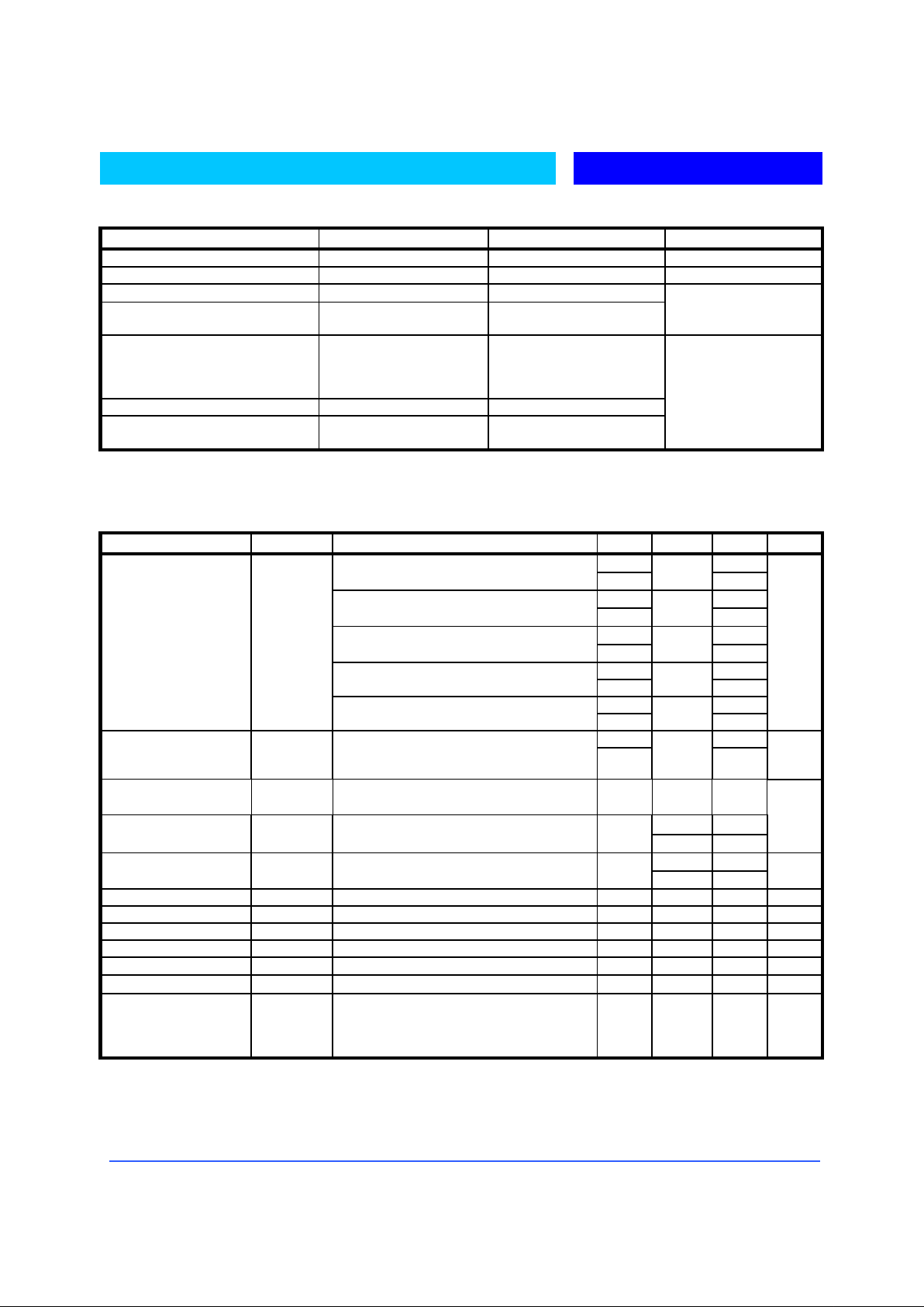
Absolute Maximum Rating
Parameter Symbol Value Unit
Maximum Input Voltage V
IN
7 V
Power Dissipation P
O
Internally Limited W
Thermal Resistance Junction to Case
θ
JC
3
Thermal Resistance Junction to
Ambient
θ
JA
50
°
C/W
Operating Junction
Temperature Range
Control Section
Power Transistor
T
J
0 to 125
0 to 150
Storage Temperature Range T
STG
-65 to 150
Lead Temperature (Soldering 10
Sec.)
T
LEAD
260
°
C
Electrical Characteristics
(VIN = 4.75V to 5.25V; IO = 10mA to 5.0Amp, unless otherwise specified)
Parameter Symbol Conditions MIN TYP MAX UNIT
1.485 1.515 V
CONT
=4V, V
PWR
=2V
V
CONT
=3V, V
PWR
=2.3V, I
LOAD
=10mA to 5A
1.475
1.5
1.525
2.475 2.525 V
CONT
=5V, V
PWR
=3.3V
V
CONT
=4V, V
PWR
=3.3V, I
LOAD
=10mA to 5A
2.460
2.5
2.540
2.970 3.030 V
CONT
=5.5V, V
PWR
=3.5V
V
CONT
=4.5V, V
PWR
=3.8V, I
LOAD
=10mA - 5A
2.950
3.0
3.050
3.267 3.333 V
CONT
=5.8V, V
PWR
=3.8V
V
CONT
=4.8V, V
PWR
=4.1V, I
LOAD
=10mA - 5A
3.247
3.3
3.353
4.950 5.050
Output Voltage V
O
V
CONT
=7.5V, V
PWR
=5.5V
V
CONT
=6.5V, V
PWR
=5.8V, I
LOAD
=10mA- 5A
4.920
5.0
5.080
V
1.238 1.262 Reference Voltage V
ref
V
CONT
=2.75V, V
PWR
=2V, I
LOAD
=10mA
V
CONT
=2.7V, to 12V
V
PWR
=3.3V to 5.5V, I
LOAD
=10mA to 5A
1.230
1.250
1.270
V
Line Regulation (1) REG
(line)
IO = 10mA, VIN =5V, T= 25 °C
0.04 0.2
0.08 0.40 Load Regulation (1) REG
(LOAD)
IO = 10mA, VIN =5V, T= 25 °C
%
0.10 0.17 Dropout Voltage V
PWR-VOUT VCONT=VOUT
+2.5V, I
LOAD
=10mA
V
CONT=VOUT
+2.5V, I
LOAD
=5A
0.55 0.70
V
Minimum lo ad Current I
min
5 10 mA
Current Limit I
S
(Vin-V
out
)=3V 5.5 6.8 A
Ground Pin Current I
Q
VIN =5V 6 10 mA
Temperature Stability T
S
IO = 10mA, VIN =5V 0.5 %
Thermal Regulation
T= 25 °C, 30ms pulse
0.003 %/W
Ripple Rejection R
A
T= 25 °C, VIN =5V
60 80 dB
Thermal Resistance - TO-220 Junction to Tab
Junction to Ambient
DD Package Junction to Tab
Junction to Ambient
3.0
60
3.0
60
3.0
60
3.0
60
°
C/W
Note:
Output Switch tests are performed under pulsed conditions to minimize power dissipation
Page 3

Bay Linear, Inc
2478 Armstrong Street, Livermore, CA 94550 Tel: (925) 606-5950, Fax: (925) 940-9556 www.baylinear.com
B1581
BLOCK DIAGRAM
PIN DESCRIPTION
1. Sense = Allows Kelvin sense of V
OUT
at the load. (Positive side of the reference voltage of the
device).
2. ADJ = Negative side of the reference voltage for the device. Adding a small bypass capacitor from
the ADJ pin to ground will improve the transient response.
3. V
OUT
= Power output of the device.
4. V
CTRL
= Supply pin for the control circuitry of the device. The current flow into this pin will be about
1% of the output current. V
CTRL
must be between 1.0V and 1.3V greater than the output voltage for
the device to regulate.
5.
V
IN
= Output load current is supplied through this pin. V
IN
must be between 0.1V and 0.8V greater
than the output voltage for the device to regulate.
(4) V
CTRL
V
IN
(5)
S.O.A
V
OUT
(3)
LIMIT
SENSE
CURRENT
LIMIT
AMPLIFIER
THERMAL OVERLOAD
VOLTAGE
REGULATION
AMPLIFIER
V
REF
SENSE (1)
ADJ (2)
Page 4

Bay Linear, Inc
2478 Armstrong Street, Livermore, CA 94550 Tel: (925) 606-5950, Fax: (925) 940-9556 www.baylinear.com
B1581
APPLICATIONS NOTES
The B1581 is designed as a high performance and low cost
solution for application requiring a lower dropout than
traditional NPN regulators.
The B1581 uses a separate input voltage V
CTRL
(V
CTRL
≥
V
OUT
+ 1.3V) to minimize the dropout voltage. This allows the
2.5V power for the load to come from a 3.3V system supply.
As added benefit this will reduce the heat dissipation, and
lower heat sink and cooling fan cost. A typical application
would use 5V for Vin and 3.3V for V
CTRL
from a motherboard
power supply to provide a nominal 2.5V output. Using the
sense pin allows to Kelvin measure the output, reducing
resistive-associated errors.
The B1581 can power the 2.5V core voltage for
microprocessors such as Pen t i um, P55C, AMD5k86 and
K6 and the IBM PowerPC 603EV and 604EV processors.
*The reduction of heat dissipation is a result of the increase of
the regulator efficiency (efficiency = V
OUT
/ VIN).
Adjustable Regulator Design
1.25V reference voltage is being developed between the
SENSE pin and the ADJ pin of the AS1581. Adding two
external resistors (see fig 1.) will allow setting the output
voltage from 1.25V to 6V. R
1
is chosen so that this
current is specified minimum lo ad cu rren t of 10 mA. R
2
is
given by the formula: V
OUT
= V
REF
(1+ R2/R1) + I
ADJ
(R2).
The current flowing from the ADJ pin is typically 50µA.
This ADJ pin contributes to the final VOUT but is usually
neglected. Connecting the sense pin to the top of the
resistor divider will improve load regulation.
Lowering Noise
Using the SENSE pin to Kelvin the load will increase
accuracy of the output vo ltage during load regulat ion. For
the fixed voltage d evices, adding a capacito r at the GND
pin will improve transient response. This capacitor is
chosen in t he range of 1µF to 0.1µF and will depend on
the amount of output capacitance in the system.
TYPICAL APPLICATION
BAY LINEAR
B1581
SENSE
ADJ
V
IN
V
CTRL
R1
124
C4
2 X 330uF
C2
10uF
C1
330uF
5V
V
CTRL
3.3V
V
IN
1
2
3
4
5
C3
.033uF
(1) V
CTRL
needed when VIN < 5V.
(2) V
OUT
= V
REF
(1 + R2/ R1) + I
ADJ
R2.
(3) V
REF
is measured across adjust to sense.
2.5V
V
OUT
Ω
R1
124
Ω
V
OUT
Fig. 1 Adjustable Regulator
Page 5

Bay Linear, Inc
2478 Armstrong Street, Livermore, CA 94550 Tel: (925) 606-5950, Fax: (925) 940-9556 www.baylinear.com
B1581
BAY LINEAR
B1581
SENSE
FIXED
V
IN
V
CTRL
C4
2 X 330uF
C2
10uF
C1
330uF
5V
V
CTRL
3.3V
V
I
N
1
2
3
4
5
C3
.
033uF
(1) V
CTRL
is needed when VIN <5V.
Fig.2 Typical Fixed Regulator
2.5V
V
OUT
V
OUT
0.405 0.005
0.055 (1.397)
0.356 0.005
±
(10.287 ±
0.127)
±
(9.042
0.127)
±
(15.24
0.635)
±
0.600 0.025
±
(1.702 0.127)
±
0.067
0.005
±
(0.813
0.076)
±
0.032 0.003
±
0.176 0.005±(4.470 0.127)
±
0.050 0.002
±
(1.270 0.051)
±
0.015
+
-
0.003
0° 8°
(0.381 0.074)
+
-
0.100
0.010
(2.540 0.254)
±
±
Page 6

Bay Linear, Inc
2478 Armstrong Street, Livermore, CA 94550 Tel: (925) 606-5950, Fax: (925) 940-9556 www.baylinear.com
B1581
TO-220-5
Advance Information
-
These data sheets contain descriptions of products that are in development. The specifications are based on the engineering calculations,
computer simulations and/ or initial prototype evaluation.
Preliminary Information
-
These data sheets contain minimum and maximum specifications that are based on the initial device characterizations. These limits are
subject to change upon the completion of the full characterization over the specified temperature and supply voltage ranges.
The application circuit examples are only to explain the representative applications of the devices and are not intended to guarantee any circuit
design or permit any industrial property right to other rights to execute. Bay Linear takes no responsibility for any problems related to any
industrial property right resulting from the use of the contents shown in the data book. Typical parameters can and do vary in different
applications. Customer’s technical experts must validate all operating parameters including “ Typical” for each customer application.
LIFE SUPPORT AND NUCLEAR POLICY
Bay Linear products are not authorized for and should not be used within life support systems which are intended for surgical
implants into the body to support or sustain life, in aircraft, space equipment, submarine, or nuclear facility applications without
the specific written consent of Bay Linear President.
0.108
+
-
0.005
(2.74
+
-
2.74)
0.400
+
-
0.005
(10.16
+
-
0.13)
0.150 D
+
-
0.005
(3.81D
+
-
0.13)
0.175
+
-
0.005
(4.45
+
-
0.13)
0.050
+
-
0.005
(1.27
+
-
0.13)
0.250
+
-
0.005
(6.35
+
-
0.13)
0.590
+
-
0.005
(14.99
+
-
0.13)
SEATING
PLANE
0.547
+
-
0.005
(13.89
+
-
0.005)
0.067
+
-
0.005
(1.70
+
-
0.127)
0.268 REF
(6.81 REF)
0.268 REF
0.032
+
-
0.005
(0.81
+
-
0.13)
0.015
+
-
0.005
(0.38
+
-
0.13)
0.105
+
-
0.005
(2.67
+
-
0.13)
1.137 REF
(28.88 REF)
7°
Typ.
 Loading...