

Datasheet B1121-Z-5.0, B1121-Z-3.3, B1121-Z-3.0, B1121-R-5.0, B1121-R-3.3 Datasheet (BAYLI)
...Page 1
Bay Linear, Inc
2478 Armstrong Street, Livermore, CA 94550 Tel: (925) 989-7144, Fax: (925) 940-9556 www.baylinear.com
150mA Low Dropout Voltage Regulator
B1121
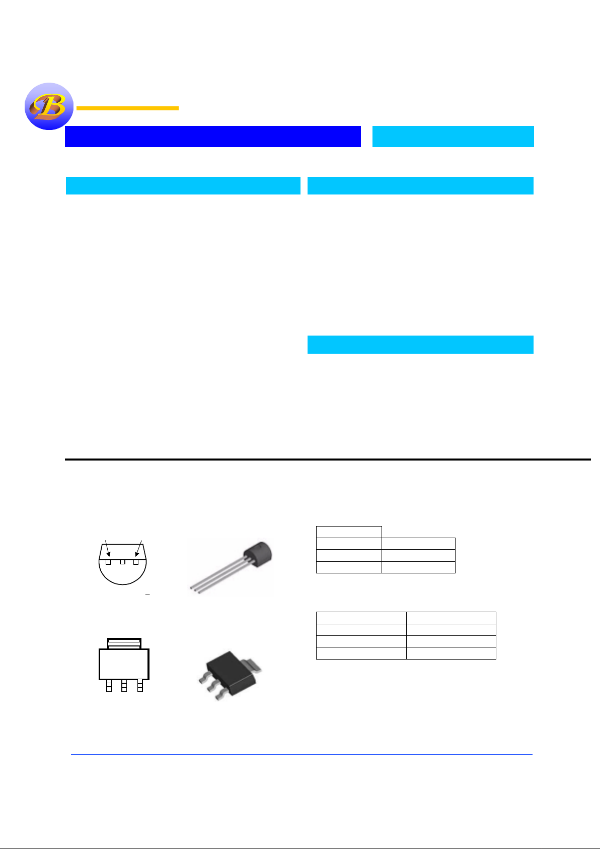
Pin Connection
TO-92 (Z)
Ordering Information
Package
1%
SOT-223
B1121-R-XX
TO-92
B1121-Z-XX
“XX” Voltage Selection Guide
Vout XX Code
5.0V
5
3.3V
3.3
3V
3
Description
The Bay Linear B1121 is a low power voltage regulator.
This device is an excellent choice for use in batterypowered applications such as cordless telephones, radio
control systems, and portable computers. The B1121
features very low quiescent current and very low
dropout voltage of 0.40 volts. This includes a tight
initial tolerance of ± 1% max, and very low output
temperature coefficient, making the B1121 useful as a
low-power voltage reference.
The B1121 feature low quiescent current ( 75µA Typ.)
and low dropout of 40mV at light loads 400mV (typ.) at
150mA.
The Bay Linear B1121 is available in fixed voltages of 3.0V,
3.3V, and 5.0V in a SOT-223 and TO-92 packages.
Features
•
1% Output Accuracy @ 3.0V, 3.3V, 5.0V
•
Very Low Quiescent Current
•
0.40V Low Dropout Voltage
•
Extremely Tight Load and Line
Regulation
•
Very Low Temperature Coefficient
• Needs only 1µµµµF for Stability
• Current & Thermal Limiting
•
Equivalent Replacement For LT1121
Applications
• Battery Powered Systems
• Portable instrumentation
• Notebooks Computers
• Potable Consumer Equipment
• Automotive electronics
• SMPS Post-Regulator
•
Bay Linear
Bay LinearBay Linear
Bay Linear
Inspire the Linear Power
Ins
p
ire the Linear PowerInspire the Linear Power
Ins
p
ire the Linear Power
Tab V
OUT
IN OUTGND
Tab V
OUT
Front View
Tab V
OUT
IN OUTGND
Tab V
OUT
Front View
Vout
Vin
Grd
SOT-223
Page 2
Bay Linear, Inc
2478 Armstrong Street, Livermore, CA 94550 Tel: (925) 989-7144, Fax: (925) 940-9556 www.baylinear.com
B1121
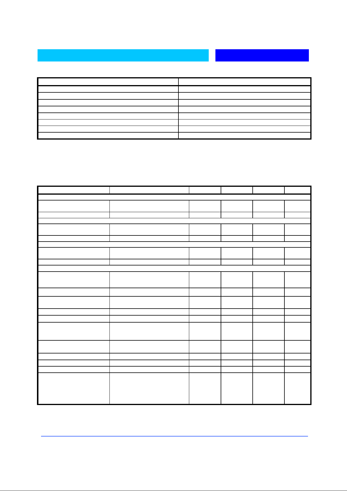
Absolute Maximum Rating
Parameter
Power Dissipation Internally Limited
Lead Temperature ( Soldering 5 seconds )
260 °C
Storage Temperature Range
-65 °C to +150 °C
Operating Junction Temperature
-55 °C to +150 °C
Input Supply Voltage -0.3V to +30V
Feedback Input Voltage -1.5V to +30V
Shutdown Input Voltage -0.3V to +30V
Error Comparator Output -0.3V to +30V
Electrical Characteristics
(VS = 15V, TA = 25°C , unless otherwise specified)
Parameter Conditions MIN TYP MAX UNIT
3.0V Version
Output Voltage
Vin=3.8V I
OUT
=1mA
V IN
≤4.3V, 1mA
≤I
L
≤ 150mA
2.97
2.955
3.00
3.00
3.03
3.045
V
Reverse Output Current B1121-3.0 V
OUT
= 3.0V, VIN = 0V 16 25
µA
3.3V Version
Output Voltage Vin=3.8V I
OUT
=1mA
V IN
≤4.3V, 1mA
≤I
L
≤ 150mA
3.250
3.20
3.30
3.30
3.35
3.366
V
Reverse Output Current B1121-3.3 V
OUT
= 3.3V, VIN = 0V 16 25
µA
5V Version
Output Voltage Vin=3.8V I
OUT
=1mA
V IN
≤4.3V, 1mA
≤I
L
≤ 150mA
4925
4.850
5.00
5.00
5.075
5.150
V
Reverse Output Current B1121-5.0 V
OUT
= 5.0V, VIN = 0V 16 25
µA
Output Voltage
-25 °C ≤ T
j
≤
85 °C
Full Operating Temperature
0.985 [ V
o
]
0.980 [ V
o
]
V
o
1.015 [ Vo ]
1.020 [ V
o
]
V
Output Voltage
100µA ≤ I
L
≤
150mA, T
j
≤ T
jmax
0.976 [Vo ] Vo 1.024 [ Vo ]
V
Output Volt age Temperatu r e
Coefficient
(Note 1) 50 150
ppm / ° C
Line Regulation (Note 3)
V
O
+ 1V ≤ VIN ≤ 30V (Note 4)
0.04 0.4 %
Load Regulation (Note 5)
100µA ≤ I
L
≤
100mA
0.1 0.3 %
Dropout Voltage
I
L
= 100µA
IL = 150mA
50
440
80
550
700
mV
Ground Current
I
L
= 100µA
I
L
= 150mA
75 8 120
14
µ
A
mA
Dropout Ground Current
V
IN
= VO - 0.5V, IL = 100µA
110 170
µ
A
Current Limit V
OUT
= 0 160 200 mA
Thermal Regulation 0.05 0.2 % / W
Output Noise,
10Hz to 100KHz
C
L
= 1µF
C
L
= 200µF
C
L
= 3.3µF
(Bypass = 0.01 µF pins 7 to 1 for
B1121-XX)
430
160
100
µ
Vrms
Page 3

Bay Linear, Inc
2478 Armstrong Street, Livermore, CA 94550 Tel: (925) 989-7144, Fax: (925) 940-9556 www.baylinear.com
B1121
Note 1:
Output or reference voltage temperature coefficients defined as the worst case voltage change divided by the total temperature range.
Note 2:
Unless otherwise specified all limits guaranteed for T
J
= 25°C, VIN = VO +1V, IL = 100µA and CL = 1µF. Additional conditions for the 8-
pin versions are feedback tied to –XX Voltage tap and output tied to output Sense pin ( V
OUT
= XX V) and V
SHUTDOWN
≤ 0.8V
Note 3:
Regulation is measured at constant junction temperature , using pulse testing with a low duty cycle. Changes in output voltage due to
heating effects are covered under specification for thermal regulation.
Note 4:
Line regulation for B1121-XX is tested at 150°C for I
L
= 1mA. For IL = 100µA and TJ = 125°C, line regulation is guaranteed by design to
0.2%. See typical performance characteristics for line regulation versus temperature and load current.
Note 5:
Dropout voltage is defined as the input to output differential at which the output voltage drops 100mV below its nominal value measured
at 1V differential. At very low values of programmed output voltage, the minimum input supply voltage of 2V (2.3V over temperature) must be
taken into account.
Note 6:
V
REF
≤ V
OUT
≤ (V
IN
–1V), 2.3V ≤ VIN ≤ 30V, 100µA ≤ IL ≤100mA, T
J
≤ T
JMAX
Note 7:
Output or reference voltage temperature coefficient is defined as the worst case voltage change divided by the total temperature range
Note 8:
Comparator thresholds are expressed in terms of a voltage differential at the feedback terminal below the nominal reference voltage
measured at V
O
+ 1V input. To express these thresholds in terms of output voltage change, multiply by the error amplifier gain = V
OUT
/ V
REF
=
(R1 + R2)/R2. For example, at a programmed ou tput voltage of 5V, the error output is guaranteed to go low when t he output drops by 95mV X
5V / 1.235V = 384mV. Thresholds remain constant as a percent of V
OUT
as V
OUT
is varied, with the dropou t warning occu rring at typic ally 5%
below nominal, 7.5% guaranteed.
Note 9:
V
SHUTDOWN
≥ 2V, VIN ≤ 30V, V
OUT
= 0, Feed-back pin tied to –XX Voltage Tap.
Page 4

Bay Linear, Inc
2478 Armstrong Street, Livermore, CA 94550 Tel: (925) 989-7144, Fax: (925) 940-9556 www.baylinear.com
B1121
APPLICATION HINTS
EXTERNAL CAPACITORS
The stability of the B1121 requires a 2.2µF or greater
capacitor between output and ground. Oscillation could
occur without this capacitor. Most types of tantalum or
aluminum electrolytic works fine here. For operations of
below -25°C solid tantalum is recommended since the
many aluminum types have electrolytes the freeze at about
-30°C. The ESR of about 5Ω or less and resonant
frequency above 500kHz are the most important
parameters in the value of the capacitor. The capacitor
value can be increased without limit.
At lower values of output current, less output capacitance
is required for stability. For the currents below 10mA the
value of the capacitor can b e reduced to 0.5µF and 0.15µF
for 1mA. More output capacitance needed for the 8-pin
version at voltages below 5V since it runs the error
amplifier at lower gain. At worst case 5µF or greater must
be used for the condition of 250mA load at 1.23V output.
The B1121, unlike other low dropout regulators will
remain stable and in regulation with no load in addition to
the internal voltage divider. This feature is especially
important in application like CMOS RAM keep-alive.
When setting the output voltage of the B1121, a minimum
load of 10mA is recommended.
If there is more than 10 inches of wire between the input
and the AC filter capacitor or if a battery is used as the
input then a 0.1µF tantalum or aluminum electrolytic
capacitor should be placed from the input to the ground.
Instability can occur if there is stray capacitance to the
B1121 feedback terminal (pin 7). This could cause more
problems when using a h igher val ue of external resistors t o
set the output voltage
This problem can be fixed by adding a 100pF capacitor
between output and feedback and increasing the output
capacitor to at least 3. 3µF.
ERROR DETECTION COMPARATOR OUTPUT
The Comparator produces a l ogic low output whenever the
B1121 output falls out of regulation by more than around
5%. This is around 60mV offset divided by the 1.235
reference voltage. This trip level remains 5% below normal
regardless of the programmed output voltage of the
regulator. Figure 1 shows the timing diagram depicting the
ERROR signal and the regulator output voltage as the
B1121 input is ramped up and down. The ERROR signal
becomes low at around 1.3V input, and goes high around 5V
input (input voltage at which Vout = 4.75). Since the
B1121’s dropout voltage is load dependent, the input
voltage trip point (around 5V) will vary with the load
current. The output voltage trip point (approx. 4.75V) does
not vary with load.
The error comparator has an open-collector output, which
requires an external pull-up resistor. Depending on the
system requirements the resistor may be returned to 5V
output or other supply voltage. In determining the value of
this resistor, note that the output is rated to sink 400µA, this
value adds to battery drain in a low battery condition.
Suggested values range from 100K to 1MΩ. If the output is
unused this resistor is not required.
PROGRAMMING THE O UTPUT VOLTAGE OF
B1121 (SO-8 Version)
The B1121 may be pin-strapped for 5V using its internal
voltage divider by tying Pin 1 (output) to Pin 2 (sense) and
Pin 7 (feedback) to Pin 6 (5V Tap).
Also, it may be programmed for any output voltage between
its 1.235V reference and its 30V maximum rating. As seen
in Figure 2, an external pair of resistors is required.
Refer to the below equation for the programming of the
output voltage::
V
OUT
= V
REF
× ( 1 + R1\ R2 )+ IFBR
1
The V
REF
is 1.235 and IFB is the feedback bias current,
nominally -20nA. The minimum recommended load current
of 1 µA forces an upper limit of 1.2 MΩ on value of R2. If
no load is presented the I
FB
produces an error of typically
2% in V
OUT
, which may be eliminated at room temperatur e
by trimming R
1
. To improve the accuracy choose the value
of R2 = 100k this reduces the error by 0.17% and increases
the resistor program current by 12µA. Since the B1121
typically draws 60 µA at no load with Pin 2 open-circuited
this is a small price to pay
+
+
+
+
4.75V
OUTPUT
VOLTAGE
ERROR*
_______
INPUT
VOLTAGE 1.3V
5.0V
Figure 1. ERROR Output Timing
_______
* See Application Info.
Page 5

Bay Linear, Inc
2478 Armstrong Street, Livermore, CA 94550 Tel: (925) 989-7144, Fax: (925) 940-9556 www.baylinear.com
B1121
REDUCING OUTPUT NOISE
It may be an advantage to reduce the AC noise present at the
output. One way is to reduce the regulator bandwidth by
increasing the size of the o utput capacito r. This is the only
way that noise can be reduced on the 3 lead B1121 but is
relatively inefficient, as increasing th e capacito r from 1µF to
220µF only decreases the noise from 430µV to 160µV
Vrms for a 100kHz bandwidth at 5V output.
Noise could also be reduced fourfold by a bypass capacitor
across R
1
, since it reduces the high frequency gain from 4 to
unity. Pick
C
BYPASS
≅
1 / 2πR
1
× 200 Hz
or choose 0.01µF. When doing this, the output capacitor
must be increased to 3.3µF to maintain stability. These
changes reduce the output noise from 430µV to 100µV
Vrms for a 100kHz bandwidth at 5V output. With the
bypass capacitor added, noise no longer scales with output
voltage so that improvements are more dramatic at higher
output voltages.
HEAT SINK REQUIREMENTS
Depending on the maximum ambient temperature and maximum
power dissipation a heat sink may be required with the B1121. The
junction temperature range has to be within the range specified
under Absolute Maximum Ratings under all possible operating
conditions. To find out if a heat sink is required, the maximum
power dissipation of the device needs to be calculated. This is the
maximum specific AC voltage that must be taken into consideration
at input. Figure 3 shows the condition and power dissipation which
should be calculated with the following formula:
P
TOTAL
= (VIN - 5) IL + (VIN)I
G
Next step is to calcu late the temperature rise T
R
(max). T
J
(max) maximum allowable junction temperature, TA (max)
maximum ambient temperature :
T
R
(max) = TJ (max) - TA (max)
Junction to ambient thermal resistance
θ
(j-A)
can be
calculated after determining of P
TOTAL & TR
(max):
θ
(J-A)
= TR (max)/P
(max)
If the
θ
(J-A)
is 60°C/W or higher, the device could be
operated without a heat sink. If the value is below 60°C/W
then the heat sink is req uired and the thermal resistance of
the heat sink can b e calcu lated b y the follo wing formula,
θ
(J-
C)
junction to case,
θ
(C-H)
case to heat sink,
θ
(H-A)
heat sink
to ambient:
θ
(J-A)
=
θ
(J-C)
+
θ
(C-H)
+
θ
(H-A)
+
2.2 uF
+
B1121
I
in
V
in
I
G
I
L
5V
IN
OUT
GND
LOAD
I
IN
= I
L
+ I
G
FIGURE 3. 5V Regulator Circuit
Page 6

Bay Linear, Inc
2478 Armstrong Street, Livermore, CA 94550 Tel: (925) 989-7144, Fax: (925) 940-9556 www.baylinear.com
B1121
TYPICAL APPLICATIONS
V
OUT
GND
+V
IN
+V
IN
*V
OUT
= 5V
2
B1121
10uF
+
B1121 FIXED +5V REGULATOR
V
OUT
GND
V
IN
B1121
R1
B1121 ADJUSTABLE REGULATOR
R2
V
OUT
GND
V
IN
B1121
R1
B1121 ADJUSTABLE REGULATOR
R2
Page 7

Bay Linear, Inc
2478 Armstrong Street, Livermore, CA 94550 Tel: (925) 989-7144, Fax: (925) 940-9556 www.baylinear.com
B1121
Package Drawing
SOT-223
0.116
0.124
0.146
0.130
0.295
0.264
0.041
0.033
0.0905 NOM
0.181 NOM
0.264
0.248
0.0040
0.0008
0.033
0.025
0.146
0.130
10°C Max
0.014
0.010
10°C
16
°
C
10°C
16
°
C
16°C
Page 8

Bay Linear, Inc
2478 Armstrong Street, Livermore, CA 94550 Tel: (925) 989-7144, Fax: (925) 940-9556 www.baylinear.com
B1121
Package Drawing
SO-8 (M)
Pin 1
1.27 (0.50)
BSC
3.8 (0.150)
4.0 (0.158)
4.6 (0.181)
5.2 (0.205)
5.8 (0.228)
6.2 (0.244)
4.8 (0.188)
5.0 (0.197)
0.49 (0.019)
0.56 (0.022)
0.35 (0.014)
0.45 (0.018)
0.10 (0.004)
0.20 (0.008)
0.19 (0.007)
0.22 (0.009)
1.35 (0.053)
1.75 (0.069)
0.61 (0.024)
0.78 (0.031)
3°-6
°
0.64 (0.025)
0.77 (0.030)
45
°
7°(4 PLCS)
7
°
(4 PLCS)
0.37 (0.015)
BSC
Page 9

Bay Linear, Inc
2478 Armstrong Street, Livermore, CA 94550 Tel: (925) 989-7144, Fax: (925) 940-9556 www.baylinear.com
B1121
PACKAGE DRAWING
TO-92(Z)
Advance Information
-
These data sheets contain descriptions of products that are in development. The specifications are based on the engineering calculations,
computer simulations and/ or initial prototype evaluation.
Preliminary Information
-
These data sheets contain minimum and maximum specifications that are based on the initial device characterizations. These limits are
subject to change upon the completion of the full characterization over the specified temperature and supply voltage ranges.
The application circuit examples are only to explain the representative applications of the devices and are not intended to guarantee any circuit
design or permit any industrial property right to other rights to execute. Bay Linear takes no responsibility for any problems related to any
industrial property right resulting from the use of the contents shown in the data book. Typical parameters can and do vary in different
applications. Customer’s technical experts must validate all operating parameters including “ Typical” for each customer application.
LIFE SUPPORT AND NUCLEAR POLICY
Bay Linear products are not authorized for and should not be used within life support systems which are intended for surgical
implants into the body to support or sustain life, in aircraft, space equipment, submarine, or nuclear facility applications without
the specific written consent of Bay Linear President.
1
2
3
0.055 (1.397)
0.045 (1.143)
0.145 (3.683)
0.135 (3.429)
10° typ.
BOTTOM VIEW
0.185 (4.699)
0.045 (1.143)
0.185 (4.699)
0.175 (4.445)
0.085 (2.159) Diameter
0.090 (2.286) typ.
Seating Plane
0.016 (0.406)
0.014 (0.356)
0.055 (1.397)
0.045 (1.143)
0.105 (2.667)
0.095 (2.413)
0.500 (12.70) Min.
0.025 (0.635) Max
Uncontrolled
Lead Diameter
5° typ.
5° typ.
0.090 (2.286) Radius typ.
0.0155 (0.3937)
0.0145 (0.3683)
 Loading...