

Datasheet B1117N-ADJ, B1117N-3.3, B1117N-2.85, B1117N-2.5, B1117N-1.8 Datasheet (BAYLI)
...Page 1
Bay Linear, Inc
2418 Armstrong Street, Livermore, CA 94550 Tel: (925) 606-5950, Fax: (925) 940-9556 www.baylinear.com
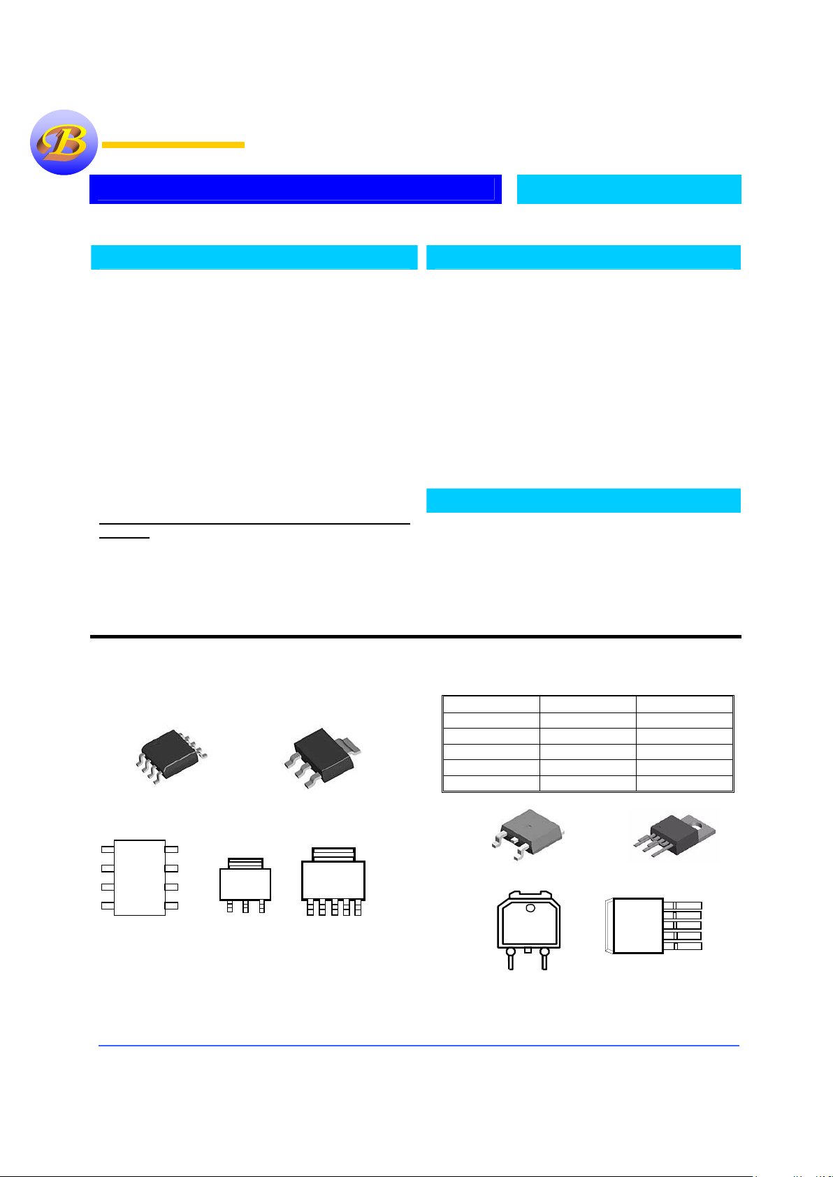
1.0Amp Low Dropout Voltage Regulator
B1117
Adjustable & Fix (0.40Volt Dropout)
Pin Connection
Ordering Information
Devices Package Temp.
B1117D-X TO-252
0 °C to 125 °C
B1117N-X TO-223
0 °C to 125 °C
B1117T-X TO-220
0 °C to 125 °C
B1117S-X TO-263
0 °C to 125 °C
B1117M-X SO-8
0 °C to 125 °C
2
1
3
4
8
7
6
5
8-Pin Surface Mount
Top View
ADJ
OUT
OUT
N.C.
IN
NC
2
1
3
4
8
7
6
5
8-Pin Surface Mount
Top View
IN
IN
2
1
3
4
8
7
6
5
8-Pin Surface Mount
Top View
ADJ
OUT
OUT
N.C.
IN
NC
2
1
3
4
8
7
6
5
8-Pin Surface Mount
Top View
IN
IN
Description
The Bay Linear B1117 is a three terminal positive NPN
regulator offered as adjustable or fix voltages of 1.5V,1.8V,
2.5V, 2.85V, 3.3V, and 5Volts. The output current has a
capability up to
1.0Amp,. This device has been optimized for
low voltage where transient response and minimum input
voltage are critical. The 2.85V version is designed specifically
to be used in active terminators for SCSI bus.
Current limit is trimmed to ensure specified output current and
controlled short-circuit current. On-Chip thermal limiting
provides protection against any combination of overload and
ambient temperatures that would create excessive junction
temperatures.
The B1117 is offered in a 3-pin SOT-223, and TO-252
(DPAK) packages compatible with other 3 terminal regulators.
5-pin version in TO-263 with lower dropout of 0.4 volt is
available.
Features
• Adjustable Output Down to 1.2V
• Output Current of 1.0Amp
• Low Dropout 1.0V for B1117
• Dropout of 0.40 V in for B1117A
• Adjustable & Fix 1.5V, 1.8V, 2.5V, 2.85V,
3.0V, 3.3V, 5.0V
• 0.05% Load Regulation
• Current & Thermal Limiting
• Lower Cost SOT-89 Package
• Available in SOT-223, and TO-252,
TO-263 & SO-8
• Similar to industry Standard LT1117
Applications
• Active SCSI terminators
• High efficiency Linear Regulator
• Post regulators fro Switching Supplies
• Battery Charger
• 5V to 3.3V linear Regulators
• Motherboard Clock Supplies
Front
TO-252
ADJ/GN
V
IN
V
OUT
1
2 3
IN
OUT Adj/GND
Tab V
OUT
Front View
SOT - 223
IN
OUT Adj/GND
Tab V
OUT
Front View
SOT - 223
V
POWER
OUTPUT
1
2
3
4
5
V
CONTROL
ADJ/GND.
SENSE
TO-263-5 Package
V
POWERVPOWER
OUTPUT
1
2
3
4
5
V
CONTROLVCONTROL
ADJ/GND.
SENSE
TO-263-5 Package
Bay Linear
Inspire the Linear Power
Tab V
OUT
SOT-223
Tab V
OUT
Front View
SOT-223 -5
4
1
5
23
#1 Sense
#2 Adj/GND
#3 OUT
#4 Control
#5 V
IN
Tab V
OUT
SOT-223
Tab V
OUT
Front View
SOT-223 -5
4
1
5
23
#1 Sense
#2 Adj/GND
#3 OUT
#4 Control
#5 V
IN
Page 2
Bay Linear, Inc
2418 Armstrong Street, Livermore, CA 94550 Tel: (925) 606-5950, Fax: (925) 940-9556 www.baylinear.com
B1117
Absolute Maximum Rating
Parameter Min Max Unit
Maximum Input Voltage 7.0 V
Operating Junction Temperature Range 0 125
Storage Temperature Range -65 150
Lead Temperature (Soldering 10 Sec.) 300
°C
Electrical Characteristics
(VIN = 7V; TJ=25°C IO = 10mA to 1.0Amp, unless otherwise specified)
Parameter Symbol Conditions MIN TYP MAX UNIT
1.238 1.250 1.262 V
1.225 1.275
Reference Voltage VO 1117-adj, I
OUT
=10mA, VIN-V
OUT
=2V, TJ=25°C
1.5V≤(V
IN-VOUT
) ≤5.75V
10mA≤I
OUT≤IFULL LOAD
-2%
1.250
+2%
V
Line Regulation (1) REG
(line)
(V
OUT
+1.5)≤VIN≤7V, I
OUT
=10mA
0.005 0.2
Load Regulation (1) REG
(LOAD)
(Vin-V
out
)=2V
10mA≤I
OUT≤IFULL LOAD
T= 25 °C
0.05 0.5
%
1117-1.8 I
OUT
=10mA, VIN=3.8V, TJ=25°C
0≤I
OUT
≤1.0Amp, 3.2V≤VIN≤7V
1.782
1.746
1.80
1.80
1.818
1.854
V
1117-2.5 I
OUT
=10mA, VIN=4.5V, TJ=25°C
0≤I
OUT
≤1.0Amp, 4.0V≤VIN≤7V
2.475
2.450
2.50
2.50
2.525
2.550
V
1117-2.85 I
OUT
=10mA, VIN=4.85V, TJ=25°C
0≤I
OUT
≤1.0Amp, 4.35V≤VIN≤7V
2.820
2.790
2.85
2.85
2.880
2.910
V
1117-3.3 I
OUT
=10mA, VIN=5.0V, TJ=25°C
0≤I
OUT
≤1.0Amp, 4.8V≤VIN≤7V
3.267
3.235
3.30
3.30
3.333
3.365
V
Output Voltage VO
1117-5.0 I
OUT
=10mA, VIN=6.0V, TJ=25°C
0≤I
OUT
≤1.0Amp, 6.5V≤VIN≤7V
4.950
4.900
5.00
5.00
5.050
5.100
V
Dropout Voltage V
D
Control Input
V
POWER=VOUT
+0.8, I
LOAD
=10mA
V
POWER=VOUT
+0.8, I
LOAD
=1.0Amp,
0.80
0.80
1.00
1.10
V
Dropout Voltage VD Power Input
V
CONTROL=VOUT
-+2.5V, I
LOAD
=1.0Amp,
0.35 0.40 V
Current Limit I
S
(Vin-V
out
)=2V
1.0 1.1 A
Minimum Load Current I
MIN LOAD
1.5V≤(VIN-V
OUT
) ≤5.75V
10 mA
Temperature Regulation T
A
T= 25 °C, 30ms pulse
0.004 0.02 %/W
Long Term Stability -
T= 25 °C, 1000Hrs
0.03 1.0 %
Temperature Stability T
S
0.5 %
Adjust pin Current -
T= 25 °C
35 120
µA
Ripple Rejection R
A
F=120Hz, C
ADJ
=22µF, C
OUT
=22µF Tantalum
I
OUT=IFULL LOAD
, (Vin-V
out
)=3V (Note 5)
60 75 dB
Thermal Shutdown 155
°C
Thermal Shutdown
Hysterics
10
°C
Thermal Resistance
Junction to case
-
SOT-223
DD Package
15
3.0
15
3.0
°C/W
Note: Output Switch tests are performed under pulsed conditions to minimize power dissipation
Page 3
Bay Linear, Inc
2418 Armstrong Street, Livermore, CA 94550 Tel: (925) 606-5950, Fax: (925) 940-9556 www.baylinear.com
B1117
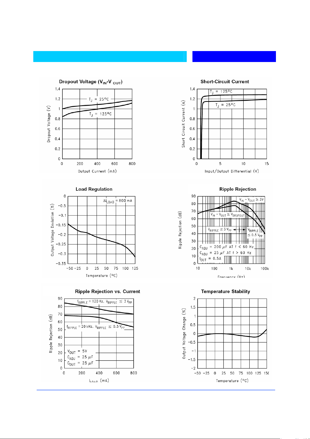
TYPICAL CHRACTRISTICS
B1117-2.85
B1117-ADJ
Page 4

Bay Linear, Inc
2418 Armstrong Street, Livermore, CA 94550 Tel: (925) 606-5950, Fax: (925) 940-9556 www.baylinear.com
B1117
TYPICAL CHRACTRISTICS (Continued)
B1117-5.0 Line Transient Response
B1117-2.85
B1117-2.85
B1117-5.0
Page 5

Bay Linear, Inc
2418 Armstrong Street, Livermore, CA 94550 Tel: (925) 606-5950, Fax: (925) 940-9556 www.baylinear.com
B1117
APPLICATION NOTES EXTERNAL
CAPACITOR
To ensure the stability of the B1117 an output capacitor of at
least 10µF (tantalum)or 50µF (aluminum) is required. The
value may change based on the application requirements on
the output load or temperature range. The capacitor
equivalent series resistance (ESR) will effect the B1117
stability. The value of ESR can vary from the type of
capacitor used in the applications. The recommended value
for ESR is 0.5Ω. The output capacitance could increase in
size to above the minimum value. The larger value of
output capacitance as high as 100µF can improve the load
transient response.
SOLDERING METHODS
The B1117 SOT-223 package is designed to be compatible
with infrared reflow or vapor-phase reflow soldering
techniques. During soldering the non-active or mildly active
fluxes may be used. The B1117 die is attached to the heat
sink lead which exits opposite the input, output, and ground
pins.
Hand soldering and wave soldering should be avoided since
these methods can cause damage to the device with
excessive thermal gradients on the package. The SOT-223
recommended soldering method are as follows: vapor phase
reflow and infrared reflow with the component preheated to
within 65°C of the soldering temperature range.
THERMAL CHARACTERISTICS
The thermal resistance of B1117 is 15°C/W from junction to
tab and 31 °C/W from tab to ambient for a total of 46 °C/W
from junction to ambient. The B1117 features the internal
thermal limiting to protect the device during overload
conditions. Special care needs to be taken during continues
load conditions the maximum junction temperature does not
exceed 125 °C.
Taking the FR-4 printed circuit board and 1/16 thick with 1
ounce copper foil as an experiment (fig.1 & fig.2), the PCB
material is effective at transmitting heat with the tab
attached to the pad area and a ground plane layer on the
backside of the substrate. Refer to table 1 for the results of
the experiment.
The thermal interaction from other components in the
application can effect the thermal resistance of the B1117.
The actual thermal resistance can be determined with
experimentation. B1117 power dissipation is calculated as
follows:
P
D
= (VIN - V
OUT
)(I
OUT
)
Maximum Junction Temperature range:
TJ = T
ambient
(max) + PD* thermal resistance (Junction-toambient)
Maximum Junction temperature must not exceed the
125°C.
10uF
+
Ω
..
27K
B1117-2.85
+
10V
10uF
2.85V
10uF
+
Ω
..
27K
B1117-2.85
+
10V
10uF
2.85V
PO = (10V - 2.85)(105mA) = (7.15)(105mA) = 750mW
Fig. 1. Circuit Layout, Thermal Experiments.
50 X 50 mm
35 X 17 mm
16 X 10 mm
Fig. 2. Substrate Layout for SOT-223
Page 6

Bay Linear, Inc
2418 Armstrong Street, Livermore, CA 94550 Tel: (925) 606-5950, Fax: (925) 940-9556 www.baylinear.com
B1117
TOTAL PC BOARD AREA TOPDIDE COPPER AREA BACKSIDE COPPER AREA THERMAL RESISTANCE
JUNCTION TO AMBIENT
2500mm
2500mm
2500mm
2500mm
2500mm
1600mm
2500mm
2500mm
1600mm
900mm
900mm
2500mm
1250mm
950mm
2500mm
1800mm
600mm
1250mm
915mm
600mm
240mm
240mm
2500mm
2500mm
2500mm
0
0
1600mm
0
0
0
900mm
0
46°C/W°
47°C/W°
49°C/W°
51°C/W°
53°C/W°
55°C/W°
58°C/W°
59°C/W°
67°C/W°
72°C/W°
85°C/W°
LOAD
ADJ
BAY
B1117
1.0Amp Current output
V
IN
C
1
R
1
OUT
IN
IN
OUT
ADJ
BAY
B1117
C
1
R
1
R
2
V
OUT
Typical Adjustable Regulator
V
IN
C
2
V
OUT
= V
REF
(1+R2/R1) +ADJ
Page 7

Bay Linear, Inc
2418 Armstrong Street, Livermore, CA 94550 Tel: (925) 606-5950, Fax: (925) 940-9556 www.baylinear.com
B1117
SOT223 Package
Advance Information- These data sheets contain descriptions of products that are in development. The specifications are based on the engineering calculations,
computer simulations and/ or initial prototype evaluation.
Preliminary Information- These data sheets contain minimum and maximum specifications that are based on the initial device characterizations. These limits are
subject to change upon the completion of the full characterization over the specified temperature and supply voltage ranges.
The application circuit examples are only to explain the representative applications of the devices and are not intended to guarantee any circuit
design or permit any industrial property right to other rights to execute. Bay Linear takes no responsibility for any problems related to any
industrial property right resulting from the use of the contents shown in the data book. Typical parameters can and do vary in different
applications. Customer’s technical experts must validate all operating parameters including “ Typical” for each customer application.
LIFE SUPPORT AND NUCLEAR POLICY
Bay Linear products are not authorized for and should not be used within life support systems which are intended for surgical
implants into the body to support or sustain life, in aircraft, space equipment, submarine, or nuclear facility applications without
the specific written consent of Bay Linear President.
0.116
0.124
0.146
0.130
0.295
0.264
0.041
0.033
0.0905 NOM
0.181 NOM
0.264
0.248
0.0040
0.0008
0.033
0.025
0.146
0.130
10°C Max
0.014
0.010
10°C
16
°
C
10°C
16
°
C
16°C
 Loading...