

Datasheet AZ10LVEL33TR2, AZ10LVEL33TR1, AZ10LVEL33T, AZ10LVEL33LR2, AZ10LVEL33LR1 Datasheet (AZMIC)
...Page 1

AZ10LVEL33
AZ100LVEL33
ECL/PECL ÷4 Divider
1630 S. STAPLEY DR., SUITE 125 • MESA, ARIZONA 85204 • USA • (480) 962-5881 • FAX (480) 890-2541
www.azmicrotek.com
ARIZONA MICROTEK, INC.
FEATURES
• Operating Range of 3.0V to 5.5V
• 470ps Propagation Delay
• 4.0GHz Toggle Frequency
• Internal Input Pulldown Resistors
• Direct Replacement for ON Semiconductor
MC10EL33, MC100EL33 and
MC100LVEL33
• Transistor Count = 91 Devices
DESCRIPTION
The AZ10/100LVEL33 is an integrated ÷4 divider. The reset pin is asynchronous and clears the output (Q
Low, Q¯ High) on the rising edge. Upon power-up, the internal flip-flop will be in a random logic state; the reset
allows for the synchronization of multiple LVEL33’s in a system.
The LVEL33 provides a V
BB
output for single-end use or a DC bias reference for AC coupling to the device.
For single-ended input applications, the V
BB
reference should be connected to one side of the CLK/ CLK ¯¯¯¯ differential
input pair. The input signal is then fed to the other CLK/ CLK ¯¯¯¯ input. The V
BB
pin can support 1.0mA sink/source
current. When used, the V
BB
pin should be bypassed to ground via a 0.01µF capacitor.
NOTE: Specifications in the ECL/PECL tables are valid when thermal equilibrium is established.
LOGIC DIAGRAM AND PINOUT ASSIGNMENT
1
4
3
2
6
5
7
8
R
÷4
Reset
CLK
V
BB
V
CC
Q
V
EE
CLK
Q
PACKAGE AVAILABILITY
PACKAGE PART NO. MARKING
MLP 16 AZ10/100LVEL33L AZML33
MLP 16 AZ10/100LVEL33LR1 AZML33
MLP 16 AZ10/100LVEL33LR2 AZML33
SOIC 8 AZ10LVEL33D AZM10LVEL33
SOIC 8 T&R AZ10LVEL33DR1 AZM10LVEL33
SOIC 8 T&R AZ10LVEL33DR2 AZM10LVEL33
SOIC 8 AZ100LVEL33D AZM100LVEL33
SOIC 8 T&R AZ100LVEL33DR1 AZM100LVEL33
SOIC 8 T&R AZ100LVEL33DR2 AZM100LVEL33
TSSOP 8 AZ10LVEL33T AZTLV33
TSSOP 8 T&R AZ10LVEL33TR1 AZTLV33
TSSOP 8 T&R AZ10LVEL33TR2 AZTLV33
TSSOP 8 AZ100LVEL33T AZHLV33
TSSOP 8 T&R AZ100LVEL33TR1 AZHLV33
TSSOP 8 T&R AZ100LVEL33TR2 AZHLV33
PIN DESCRIPTION
PIN FUNCTION
CLK, CLK¯¯¯ Clock Inputs
Reset Asynch Reset
VBB Reference Voltage Output
Q, Q¯ Data Outputs
V
CC
Positive Supply
V
EE
Negative Supply
Page 2
AZ10LVEL33
AZ100LVEL33
March 2002 * REV - 1 www.azmicrotek.com
2
Absolute Maximum Ratings are those values beyond which device life may be impaired.
Symbol Characteristic Rating Unit
VCC PECL Power Supply (VEE = 0V) 0 to +8.0 Vdc
VI PECL Input Voltage (V
EE
= 0V) 0 to +6.0 Vdc
VEE ECL Power Supply (VCC = 0V) -8.0 to 0 Vdc
VI ECL Input Voltage (VCC = 0V) -6.0 to 0 Vdc
I
OUT
Output Current --- Continuous
--- Surge
50
100
mA
TA Operating Temperature Range -40 to +85
°C
T
STG
Storage Temperature Range -65 to +150
°C
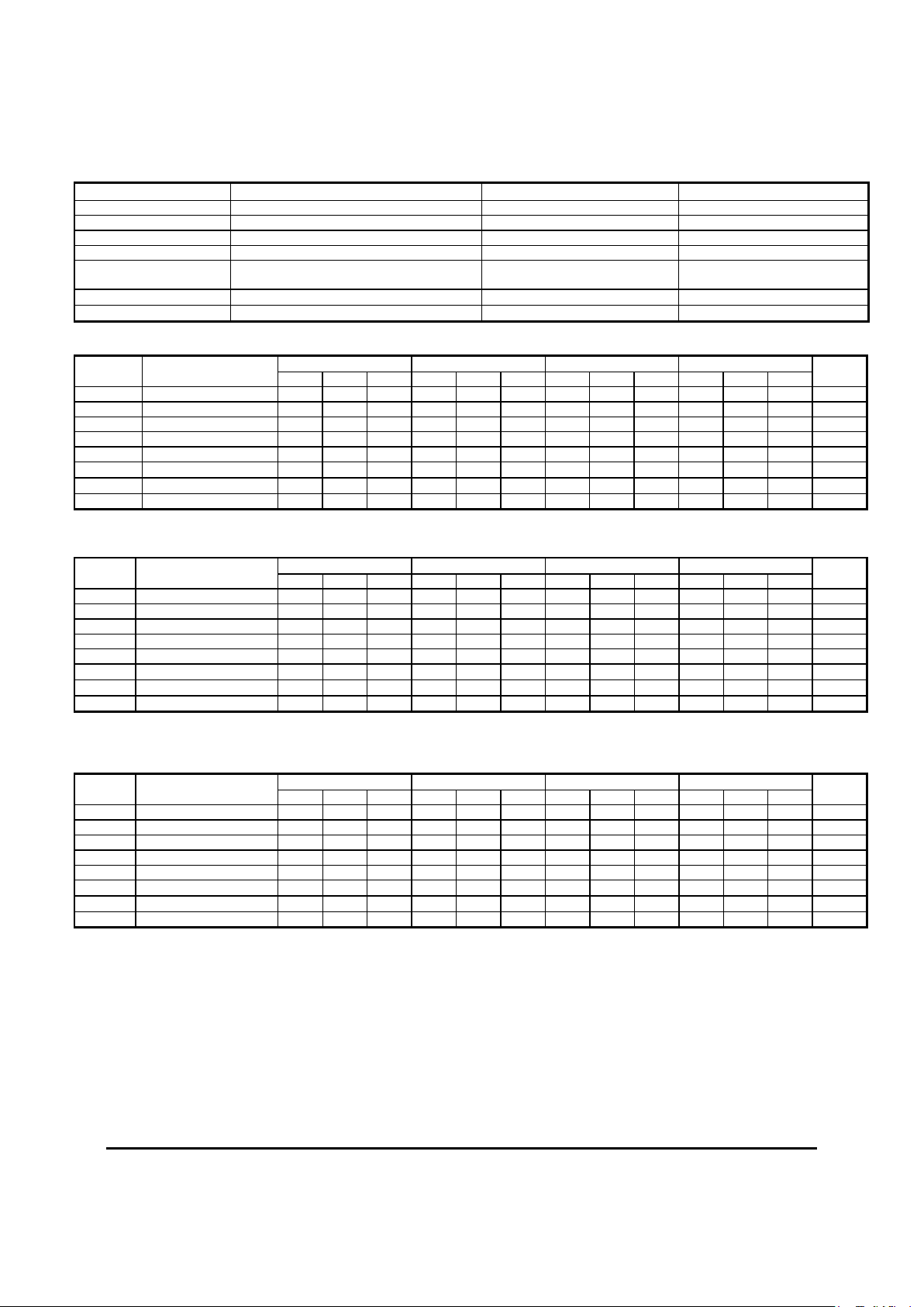
10K ECL DC Characteristics (VEE = -3.0V to -5.5V, VCC = GND)
-40°C 0°C 25°C 85°C
Symbol Characteristic
Min Typ Max Min Typ Max Min Typ Max Min Typ Max
Unit
VOH Output HIGH Voltage1 -1080 -890 -1020 -840 -980 -810 -910 -720 mV
VOL Output LOW Voltage1 -1950 -1650 -1950 -1630 -1950 -1630 -1950 -1595 mV
VIH Input HIGH Voltage -1230 -890 -1170 -840 -1130 -810 -1060 -720 mV
VIL Input LOW Voltage -1950 -1500 -1950 -1480 -1950 -1480 -1950 -1445 mV
VBB Reference Voltage -1430 -1300 -1380 -1270 -1350 -1250 -1310 -1190 mV
IIL
Input LOW Current -150 -150 -150 -150
µA
IIH
Input HIGH Current 150 150 150 150
µA
IEE Power Supply Current 27 33 27 33 27 33 27 33 mA
1. Each output is terminated through a 50Ω resistor to VCC – 2V.
10K LVPECL DC Characteristics (VEE = GND, VCC = +3.3V)
-40°C 0°C 25°C 85°C
Symbol Characteristic
Min T
yp
Max Min T
yp
Max Min T
yp
Max Min T
yp
Max
Unit
VOH Output HIGH Voltage
1,2
2220 2410 2280 2460 2320 2490 2390 2580 mV
VOL Output LOW Voltage
1,2
1350 1650 1350 1670 1350 1670 1350 1705 mV
VIH Input HIGH Voltage1 2070 2410 2130 2460 2170 2490 2240 2580 mV
VIL Input LOW Voltage1 1350 1800 1350 1820 1350 1820 1350 1855 mV
VBB Reference Voltage1 1870 2000 1920 2030 1950 2050 1990 2110 mV
IIL
Input LOW Current -150 -150 -150 -150
µA
IIH Input HIGH Current 150 150 150 150
µA
IEE Power Supply Current 27 33 27 33 27 33 27 33 mA
1. For supply voltages other that 3.3V, use the ECL table values and ADD supply voltage value.
2. Each output is terminated through a 50Ω resistor to V
CC
– 2V.
10K PECL DC Characteristics (VEE = GND, VCC = +5.0V)
-40°C 0°C 25°C 85°C
Symbol Characteristic
Min T
yp
Max Min T
yp
Max Min T
yp
Max Min T
yp
Max
Unit
VOH Output HIGH Voltage
1,2
3920 4110 3980 4160 4020 4190 4090 4280 mV
VOL Output LOW Voltage
1,2
3050 3350 3050 3370 3050 3370 3050 3405 mV
VIH Input HIGH Voltage1 3770 4110 3830 4160 3870 4190 3940 4280 mV
VIL Input LOW Voltage1 3050 3500 3050 3520 3050 3520 3050 3555 mV
VBB Reference Voltage1 3570 3700 3620 3730 3650 3750 3690 3810 mV
IIL
Input LOW Current -150 -150 -150 -150
µA
IIH Input HIGH Current 150 150 150 150
µA
IEE Power Supply Current 27 33 27 33 27 33 27 33 mA
1. For supply voltages other that 5.0V, use the ECL table values and ADD supply voltage value.
2. Each output is terminated through a 50Ω resistor to V
CC
– 2V.
Page 3
AZ10LVEL33
AZ100LVEL33
March 2002 * REV - 1 www.azmicrotek.com
3
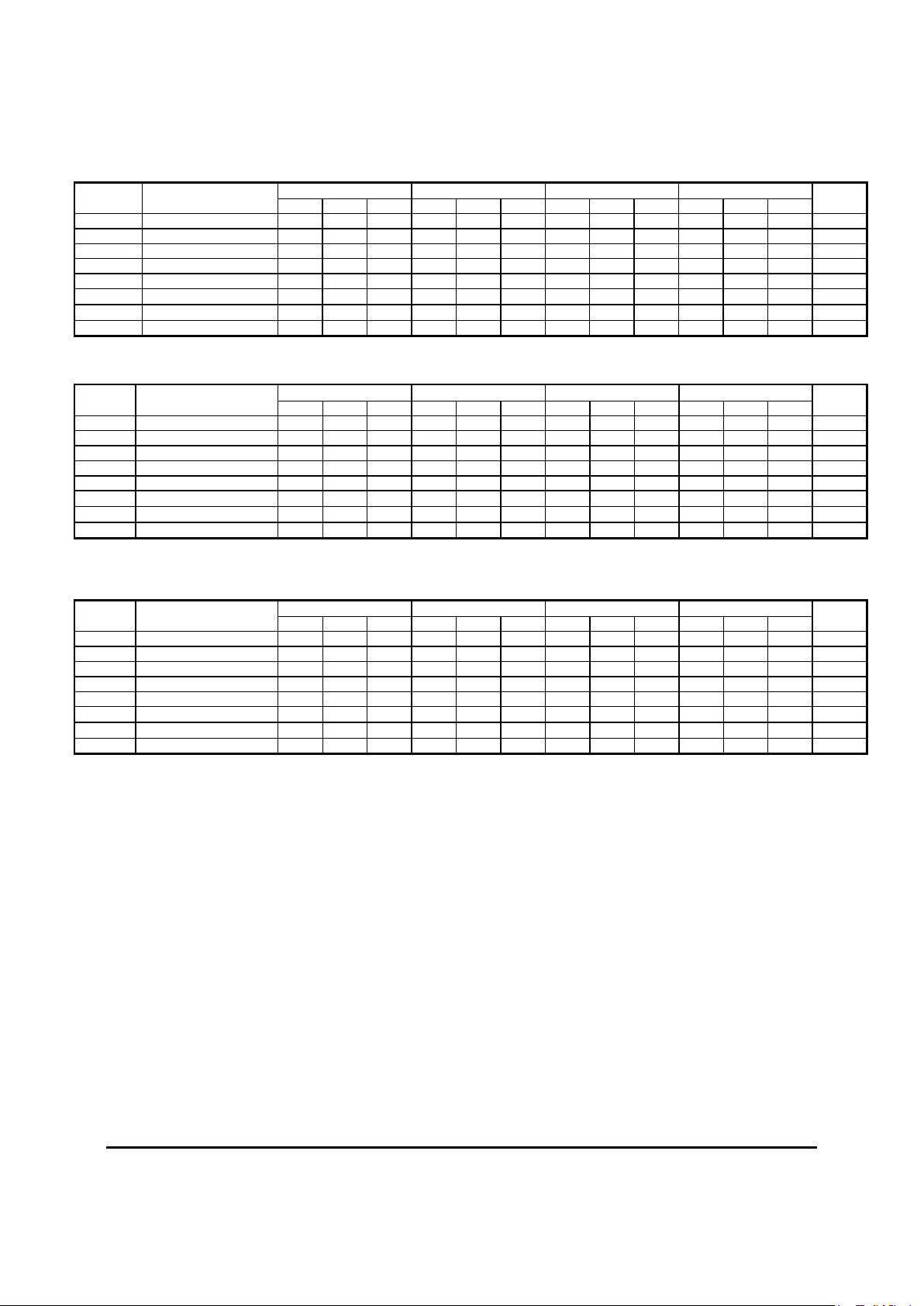
100K ECL DC Characteristics (V
EE
= -3.0V to -5.5V, VCC = GND)
-40°C 0°C 25°C 85°C
Symbol Characteristic
Min Typ Max Min Typ Max Min Typ Max Min Typ Max
Unit
VOH Output HIGH Voltage1 -1085 -1005 -880 -1025 -955 -880 -1025 -955 -880 -1025 -955 -880 mV
VOL Output LOW Voltage1 -1830 -1695 -1555 -1810 -1705 -1620 -1810 -1705 -1620 -1810 -1705 -1620 mV
VIH Input HIGH Voltage -1165 -880 -1165 -880 -1165 -880 -1165 -880 mV
VIL Input LOW Voltage -1810 -1475 -1810 -1475 -1810 -1475 -1810 -1475 mV
VBB Reference Voltage -1380 -1260 -1380 -1260 -1380 -1260 -1380 -1260 mV
IIL
Input LOW Current -150 -150 -150 -150
µA
IIH
Input HIGH Current 150 150 150 150
µA
IEE Power Supply Current 27 33 27 33 27 33 31 37 mA
1. Each output is terminated through a 50Ω resistor to VCC – 2V.
100K LVPECL DC Characteristics (VEE = GND, VCC = +3.3V)
-40°C 0°C 25°C 85°C
Symbol Characteristic
Min T
yp
Max Min T
yp
Max Min T
yp
Max Min T
yp
Max
Unit
VOH Output HIGH Voltage
1,2
2215 2295 2420 2275 2345 2420 2275 2345 2420 2275 2345 2420 mV
VOL Output LOW Voltage
1,2
1470 1605 1745 1490 1595 1680 1490 1595 1680 1490 1595 1680 mV
VIH Input HIGH Voltage1 2135 2420 2135 2420 2135 2420 2135 2420 mV
VIL Input LOW Voltage1 1490 1825 1490 1825 1490 1825 1490 1825 mV
VBB Reference Voltage1 1920 2040 1920 2040 1920 2040 1920 2040 mV
IIL
Input LOW Current -150 -150 -150 -150
µA
IIH Input HIGH Current 150 150 150 150
µA
IEE Power Supply Current 27 33 27 33 27 33 31 37 mA
1. For supply voltages other that 3.3V, use the ECL table values and ADD supply voltage value.
2. Each output is terminated through a 50Ω resistor to V
CC
– 2V.
100K PECL DC Characteristics (VEE = GND, VCC = +5.0V)
-40°C 0°C 25°C 85°C
Symbol Characteristic
Min T
yp
Max Min T
yp
Max Min T
yp
Max Min T
yp
Max
Unit
VOH Output HIGH Voltage
1,2
3915 3995 4120 3975 4045 4120 3975 4045 4120 3975 4045 4120 mV
VOL Output LOW Voltage
1,2
3170 3305 3445 3190 3295 3380 3190 3295 3380 3190 3295 3380 mV
VIH Input HIGH Voltage1 3835 4120 3835 4120 3835 4120 3835 4120 mV
VIL Input LOW Voltage1 3190 3525 3190 3525 3190 3525 3190 3525 mV
VBB Reference Voltage1 3620 3740 3620 3740 3620 3740 3620 3740 mV
IIL
Input LOW Current -150 -150 -150 -150
µA
IIH Input HIGH Current 150 150 150 150
µA
IEE Power Supply Current 27 33 27 33 27 33 31 37 mA
1. For supply voltages other that 5.0V, use the ECL table values and ADD supply voltage value.
2. Each output is terminated through a 50Ω resistor to V
CC
– 2V.
Page 4

AZ10LVEL33
AZ100LVEL33
March 2002 * REV - 1 www.azmicrotek.com
4
AC Characteristics (V
EE
= -3.0V to -5.5V; VCC = GND or V
EE
= GND; VCC = +3.0V to +5.5V)
-40°C 0°C 25°C 85°C
Symbol Characteristic
Min Typ Max Min Typ Max Min Typ Max Min Typ Max
Unit
f
max
Maximum Toggle
Frequency
3.4 4.0 3.8 4.0 3.8 4.0 3.8 4.0 GHz
t
PLH
/ t
PHL
Propagation Delay
CLK to Q
Reset to Q
360
310
450
460
540
610
320
340
460
460
550
580
380
360
470
460
560
560
400
380
490
480
580
580
ps
tRR Reset Recovery 300 300 300 300 ps
t
skew
Within-Device Skew 20 20 20 20 ps
V
PP
(AC) Minimum Input Swing1 150 150 150 150 mV
V
CMR
Common Mode Range
2
Vpp < 500mV
Vpp ≥ 500mV
V
EE
+
1.2
1.4
VCC -
0.4
0.4
VEE +
1.1
1.3
VCC -
0.4
0.4
VEE +
1.1
1.3
VCC -
0.4
0.4
VEE +
1.1
1.3
VCC -
0.4
0.4
V
tr / tf
Output Rise/Fall Times
Q (20% - 80%)
100 260 100 260 100 260 100 260 ps
1. VPP is the minimum peak-to-peak differential input swing for which AC parameters are guaranteed.
2. The V
CMR
range is referenced to the most positive side of the differential input signal. Normal operation is obtained if the HIGH level falls within
the specified range and peak to peak voltage lies between V
PP
(min) and 1V.
CLK
RESET
Q
Figure 1. Timing Diagram
CLK
RESET
NC
V
EE
Q
4
3
2
1
58
7
6
10
9
12
11
NC
CLK
NC
131415
16
NC
NC
NC
NC
10K
16MLP
Q
V
CC
V
BB
Page 5

AZ10LVEL33
AZ100LVEL33
March 2002 * REV - 1 www.azmicrotek.com
5
MILLIMETERS INCHES
DIM
MIN MAX MIN MAX
A
1.75 0.069
A1
0.10 0.25 0.004 0.010
A2
1.25 1.45 0.049 0.057
A3
0.25 0.01
bp
0.36 0.49 0.014 0.019
c
0.19 0.25 0.0075 0.0100
D
4.8 5.0 0.19 0.20
E
3.8 4.0 0.15 0.16
e
1.27 0.050
HE
5.80 6.20 0.228 0.244
L
1.05 0.041
Lp
0.40 1.00 0.016 0.039
Q
0.60 0.70 0.024 0.028
v
0.25 0.01
w
0.25 0.01
y
0.10 0.004
Z
0.30 0.70 0.012 0.028
θ
0
O
8
O
0
O
8
O
N
OTES:
1. DIMENSIONS D AND E DO NOT
INCLUDE MOLD PROTRUSION.
2. MAXIMUM MOLD PROTRUSION
FOR D IS 0.15mm.
3. MAXIMUM MOLD PROTRUSION
FOR E IS 0.25mm.
PACKAGE DIAGRAM
SOIC 8
Page 6

AZ10LVEL33
AZ100LVEL33
March 2002 * REV - 1 www.azmicrotek.com
6
PACKAGE DIAGRAM
TSSOP 8
MILLIMETERS
DIM
MIN MAX
A
1.10
A1
0.05 0.15
A2
0.80 0.95
A3
0.25
bp
0.25 0.45
c
0.15 0.28
D
2.90 3.10
E
2.90 3.10
e
0.65
HE
4.70 5.10
L
0.94
Lp
0.40 0.70
v
0.10
w
0.10
y
0.10
Z
0.35 0.70
θ
0
O
6
O
N
OTES:
1. DIMENSIONS D AND E DO NOT
INCLUDE MOLD PROTRUSION.
2. MAXIMUM MOLD PROTRUSION
FOR D IS 0.15mm.
3. MAXIMUM MOLD PROTRUSION
FOR E IS 0.25mm.
Page 7

AZ10LVEL33
AZ100LVEL33
March 2002 * REV - 1 www.azmicrotek.com
7
N
OTES
1. DIMENSIONING AND TOLERANCING
CONFORM TO ASME T14-1994.
2. THE TERMINAL #1 AND PAD
NUMBERING CONVENTION SHALL
CONFORM TO JESD 95-1 SPP-012.
3. DIMENSION b APPLIES TO METALLIZED
PAD AND IS MEASURED BETWEEN 0.25
AND 0.30mm FROM PAD TIP.
4. COPLANARITY APPLIES TO THE
EXPOSED PAD AS WELL AS THE
TERMINALS.
MILLIMETERS
DIM
MIN MAX
A
0.80 1.00
A1
0.00 0.05
A3
0.25 REF
b
0.18 0.30
D
2.90 3.10
D2
0.25 1.95
E
2.90 3.10
E2
0.25 1.95
e
0.50 BSC
L
0.30 0.50
aaa
0.25
bbb
0.10
ccc
0.10
PACKAGE DIAGRAM
MLP 16
Page 8

AZ10LVEL33
AZ100LVEL33
March 2002 * REV - 1 www.azmicrotek.com
8
Arizona Microtek, Inc. reserves the right to change circuitry and specifications at any time without prior notice. Arizona Microtek, Inc.
makes no warranty, representation or guarantee regarding the suitability of its products for any particular purpose, nor does Arizona
Microtek, Inc. assume any liability arising out of the application or use of any product or circuit and specifically disclaims any and all
liability, including without limitation special, consequential or incidental damages. Arizona Microtek, Inc. does not convey any license
rights nor the rights of others. Arizona Microtek, Inc. products are not designed, intended or authorized for use as components in systems
intended to support or sustain life, or for any other application in which the failure of the Arizona Microtek, Inc. product could create a
situation where personal injury or death may occur. Should Buyer purchase or use Arizona Microtek, Inc. products for any such
unintended or unauthorized application, Buyer shall indemnify and hold Arizona Microtek, Inc. and its officers, employees, subsidiaries,
affiliates, and distributors harmless against all claims, costs, damages, and expenses, and reasonable attorney fees arising out of, directly
or indirectly, any claim of personal injury or death associated with such unintended or unauthorized use, even if such claim alleges tha
t
Arizona Microtek, Inc. was negligent regarding the design or manufacture of the part.
 Loading...