

Datasheet AZ10LVEL16VSTR2, AZ10LVEL16VSTR1, AZ10LVEL16VST, AZ10LVEL16VSDR2, AZ10LVEL16VSDR1 Datasheet (AZMIC)
...Page 1

AZ10LVEL16VS
AZ100LVEL16VS
ECL/PECL Differential Receiver with Variable Output Swing
1630 S. STAPLEY DR., SUITE 125 • MESA, ARIZONA 85204 • USA • (480) 962-5881 • FAX (480) 890-2541
www.azmicrotek.com
ARIZONA MICROTEK, INC.
FEATURES
• 250ps Propagation Delay
• High Bandwidth Output Transitions
• Operating Range of 3.0V to 5.5V
• Internal Input Pulldown Resistors
• Functionally Equivalent to ON
Semiconductor MC10EL16, MC100EL16
& MC100LVEL16
• Variable Output Swing
DESCRIPTION
The AZ10/100LVEL16VS is a differential receiver with variable output swing. The LVEL16VS has
functionality and output transition times similar to the EL16, with an input that controls the amplitude of the Q/Q¯
outputs.
The operational range of the LVEL16VS control input, V
CTRL
, is from VBB (full swing) to VCC (min. swing).
Maximum swing is achieved by leaving the V
CTRL
pin open or by tying it to the negative supply (VEE). Simple
control of the output swing can be obtained by a variable resistor between the V
BB
and VCC pins, with the wiper
driving V
CTRL
. Typical application circuits and results are described in this Data Sheet.
The LVEL16VS provides a V
BB
output for single-ended use or a DC bias reference for AC coupling to the
device. For single-ended input applications, the V
BB
reference should be connected to one side of the D/D¯
differential input pair. The input signal is then fed to the other D/D¯ input. The V
BB
pin can support 1.5mA
sink/source current. When used, the V
BB
pin should be bypassed to ground via a 0.01µF capacitor.
Under open input conditions internal input clamps will force the Q output LOW.
NOTE: Specifications in the ECL/PECL tables are valid when thermal equilibrium is established.
PACKAGE AVAILABILITY
PACKAGE PART NO. MARKING
SOIC 8 AZ10LVEL16VSD AZM10LVEL16VS
SOIC 8 T&R AZ10LVEL16VSDR1 AZM10LVEL16VS
SOIC 8 T&R AZ10LVEL16VSDR2 AZM10LVEL16VS
SOIC 8 AZ100LVEL16VSD AZM100LVEL16VS
SOIC 8 T&R AZ100LVEL16VSDR1 AZM100LVEL16VS
SOIC 8 T&R AZ100LVEL16VSDR2 AZM100LVEL16VS
TSSOP 8 AZ10LVEL16VST AZTL16VS
TSSOP 8 T&R AZ10LVEL16VSTR1 AZTL16VS
TSSOP 8 T&R AZ10LVEL16VSTR2 AZTL16VS
TSSOP 8 AZ100LVEL16VST AZHL16VS
TSSOP 8 T&R AZ100LVEL16VSTR1 AZHL16VS
TSSOP 8 T&R AZ100LVEL16VSTR2 AZHL16VS
Page 2
AZ10LVEL16VS
AZ100LVEL16VS
October 2001 * REV - 0 www.azmicrotek.com
2
Absolute Maximum Ratings are those values beyond which device life may be impaired.
Symbol Characteristic Rating Unit
VCC PECL Power Supply (VEE = 0V) 0 to +8.0 Vdc
VI PECL Input Voltage (V
EE
= 0V) 0 to +6.0 Vdc
VEE ECL Power Supply (VCC = 0V) -8.0 to 0 Vdc
VI ECL Input Voltage (VCC = 0V) -6.0 to 0 Vdc
I
OUT
Output Current --- Continuous
--- Surge
50
100
mA
TA Operating Temperature Range -40 to +85
°C
T
STG
Storage Temperature Range -65 to +150
°C
10K ECL DC Characteristics (VEE = -3.0V to -5.5V, VCC = GND)
-40°C 0°C 25°C 85°C
Symbol Characteristic
Min Typ Max Min Typ Max Min Typ Max Min Typ Max
Unit
VOH Output HIGH Voltage2 -1080 -890 -1020 -840 -980 -810 -910 -720 mV
VOL
Output LOW Voltage
2
V
CTRL
= V
BB
1
-1950 -1650 -1950 -1630 -1950 -1630 -1950 -1595 mV
VOL
Output LOW Voltage
2
V
CTRL
= V
CC
-1220 -1030 -1200 -1020 -1190 -1150 -1020 -1190 -1000 mV
VIH Input HIGH Voltage -1230 -890 -1170 -840 -1130 -810 -1060 -720 mV
VIL Input LOW Voltage -1950 -1500 -1950 -1480 -1950 -1480 -1950 -1445 mV
VBB Reference Voltage -1450 -1300 -1400 -1270 -1370 -1250 -1330 -1190 mV
IIH
Input HIGH Current
D, D¯
V
CTRL
150
40
150
40
150
40
150
40
µA
IIL
Input LOW Current
D, D¯
V
CTRL
-150
0.5
-150
0.5
-150
0.5
-150
0.5
µA
IEE Power Supply Current 18 25 18 25 18 25 21 26 mA
1. If V
CTRL
is Open Circuit, use the VOH (Max & Min) and VOL (V
CTRL
= VBB : Max only) limits.
2. Each output is terminated through a 50Ω resistor to V
CC
– 2V.
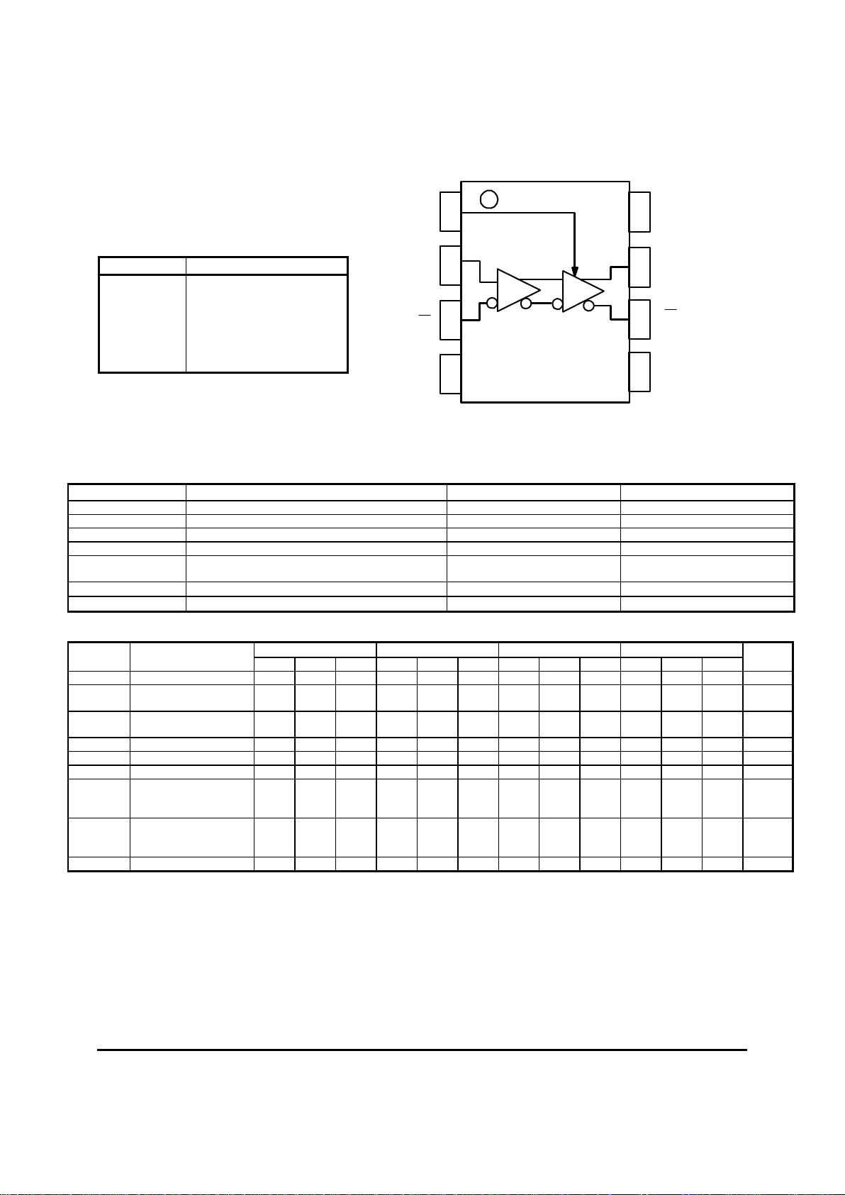
8
5
6
7
4
3
2
1
V
CC
D
V
EE
Q
Q
V
BB
D
V
CTRL
LOGIC DIAGRAM AND PINOUT ASSIGNMENT
PIN DESCRIPTION
PIN FUNCTION
D, D¯ Data Inputs
V
CTRL
Output Swing Control
Q, Q¯ Data Outputs
VBB Reference Voltage Output
VCC Positive Supply
V
EE
Negative Supply
Page 3
AZ10LVEL16VS
AZ100LVEL16VS
October 2001 * REV - 0 www.azmicrotek.com
3
10K LVPECL DC Characteristics (V
EE
= GND, VCC = +3.3V)
-40°C 0°C 25°C 85°C
Symbol Characteristic
Min T
yp
Max Min T
yp
Max Min T
yp
Max Min T
yp
Max
Unit
VOH Output HIGH Voltage
1,3
2220 2410 2280 2460 2320 2490 2390 2580 mV
VOL
Output LOW Voltage
1,3
V
CTRL
= V
BB
2
1350 1650 1350 1670 1350 1670 1350 1705 mV
VOL
Output LOW Voltage
1,3
V
CTRL
= V
CC
2080 2270 2100 2280 2110 2150 2280 2110 2300 mV
VIH Input HIGH Voltage1 2070 2410 2130 2460 2170 2490 2240 2580 mV
VIL Input LOW Voltage1 1350 1800 1350 1820 1350 1820 1350 1855 mV
VBB Reference Voltage1 1850 2000 1900 2030 1930 2050 1970 2110 mV
IIH
Input HIGH Current
D, D¯
V
CTRL
150
40
150
40
150
40
150
40
µA
IIL
Input LOW Current
D, D¯
V
CTRL
-150
0.5
-150
0.5
-150
0.5
-150
0.5
µA
IEE Power Supply Current 18 25 18 25 18 25 21 26 mA
1. For supply voltages other that 3.3V, use the ECL table values and ADD supply voltage value.
2. If V
CTRL
is Open Circuit, use the VOH (Max & Min) and VOL (V
CTRL
= VBB : Max only) limits.
3. Each output is terminated through a 50Ω resistor to V
CC
– 2V.
10K PECL DC Characteristics (V
EE
= GND, VCC = +5.0V)
-40°C 0°C 25°C 85°C
Symbol Characteristic
Min T
yp
Max Min T
yp
Max Min T
yp
Max Min T
yp
Max
Unit
VOH Output HIGH Voltage
1,3
3920 4110 3980 4160 4020 4190 4090 4280 mV
VOL
Output LOW Voltage
1,3
V
CTRL
= V
BB
2
3050 3350 3050 3350 3050 3350 3050 3405 mV
VOL
Output LOW Voltage
1,3
V
CTRL
= V
CC
3780 3970 3800 3980 3810 3850 3980 3810 4000 mV
VIH Input HIGH Voltage1 3770 4110 3830 4160 3870 4190 3940 4280 mV
VIL Input LOW Voltage1 3050 3500 3050 3520 3050 3520 3050 3555 mV
VBB Reference Voltage1 3550 3700 3600 3730 3630 3750 3670 3810 V
IIH
Input HIGH Current
D, D¯
V
CTRL
150
40
150
40
150
40
150
40
µA
IIL
Input LOW Current
D, D¯
V
CTRL
-150
0.5
-150
0.5
-150
0.5
-150
0.5
µA
IEE Power Supply Current 18 25 18 25 18 25 21 26 mA
1. For supply voltages other that 5.0V, use the ECL table values and ADD supply voltage value.
2. If V
CTRL
is Open Circuit, use the VOH (Max & Min) and VOL (V
CTRL
= VBB : Max only) limits.
3. Each output is terminated through a 50Ω resistor to V
CC
– 2V.
100K ECL DC Characteristics (VEE = -3.0V to -5.5V, VCC = GND)
-40°C 0°C 25°C 85°C
Symbol Characteristic
Min Typ Max Min Typ Max Min Typ Max Min Typ Max
Unit
VOH Output HIGH Voltage2 -1085 -1005 -880 -1025 -955 -880 -1025 -955 -880 -1025 -955 -880 mV
VOL
Output LOW Voltage
2
V
CTRL
= V
BB
1
-1890 -1620 -1870 -1680 -1870 -1775 -1680 -1870 -1680 mV
VOL
Output LOW Voltage
2
V
CTRL
= V
CC
-1180 -975 -1135 -990 -1135 -1065 -990 -1135 -990 mV
VIH Input HIGH Voltage -1165 -880 -1165 -880 -1165 -880 -1165 -880 mV
VIL Input LOW Voltage -1810 -1475 -1810 -1475 -1810 -1475 -1810 -1475 mV
VBB Reference Voltage -1420 -1260 -1420 -1260 -1420 -1260 -1420 -1260 mV
IIH
Input HIGH Current
D, D¯
V
CTRL
150
40
150
40
150
40
150
40
µA
IIL
Input LOW Current
D, D¯
V
CTRL
-150
0.5
-150
0.5
-150
0.5
-150
0.5
µA
IEE Power Supply Current 18 25 18 25 18 25 21 26 mA
1. If V
CTRL
is Open Circuit, use the VOH (Max & Min) and VOL (V
CTRL
= VBB : Max only) limits.
2. Each output is terminated through a 50Ω resistor to V
CC
– 2V.
Page 4

AZ10LVEL16VS
AZ100LVEL16VS
October 2001 * REV - 0 www.azmicrotek.com
4
100K LVPECL DC Characteristics (V
EE
= GND, VCC = +3.3V)
-40°C 0°C 25°C 85°C
Symbol Characteristic
Min T
yp
Max Min T
yp
Max Min T
yp
Max Min T
yp
Max
Unit
VOH Output HIGH Voltage
1,3
2215 2295 2420 2275 2345 2420 2275 2345 2420 2275 2345 2420 mV
VOL
Output LOW Voltage
1,3
V
CTRL
= V
BB
2
1410 1680 1430 1620 1430 1525 1620 1430 1620 mV
VOL
Output LOW Voltage
1,3
V
CTRL
= V
CC
2120 2325 2165 2310 2165 2235 2310 2165 2310
mV
VIH Input HIGH Voltage1 2135 2420 2135 2420 2135 2420 2135 2420 mV
VIL Input LOW Voltage1 1490 1825 1490 1825 1490 1825 1490 1825 mV
VBB Reference Voltage1 1880 2040 1880 2040 1880 2040 1880 2040 mV
IIH
Input HIGH Current
D, D¯
V
CTRL
150
40
150
40
150
40
150
40
µA
IIL
Input LOW Current
D, D¯
V
CTRL
-150
0.5
-150
0.5
-150
0.5
-150
0.5
µA
IEE Power Supply Current 18 25 18 25 18 25 21 26 mA
1. For supply voltages other that 3.3V, use the ECL table values and ADD supply voltage value.
2. If V
CTRL
is Open Circuit, use the VOH (Max & Min) and VOL (V
CTRL
= VBB : Max only) limits.
3. Each output is terminated through a 50Ω resistor to V
CC
– 2V.
100K PECL DC Characteristics (V
EE
= GND, VCC = +5.0V)
-40°C 0°C 25°C 85°C
Symbol Characteristic
Min T
yp
Max Min T
yp
Max Min T
yp
Max Min T
yp
Max
Unit
VOH Output HIGH Voltage
1,3
3915 3995 4120 3975 4045 4120 3975 4045 4120 3975 4045 4120 mV
VOL
Output LOW Voltage
1,3
V
CTRL
= V
BB
2
3110 3380 3130 3320 3130 3225 3320 3130 3320 mV
VOL
Output LOW Voltage
1,3
V
CTRL
= V
CC
3820 4025 3865 4010 3865 3935 4010 3865 4010 mV
VIH Input HIGH Voltage1 3820 4025 3865 4010 3865 3935 4010 3865 4010 mV
VIL Input LOW Voltage1 3835 4120 3835 4120 3835 4120 3835 4120 mV
VBB Reference Voltage1 3580 3740 3580 3740 3580 3740 3580 3740 V
IIH
Input HIGH Current
D, D¯
V
CTRL
150
40
150
40
150
40
150
40
µA
IIL
Input LOW Current
D, D¯
V
CTRL
-150
0.5
-150
0.5
-150
0.5
-150
0.5
µA
IEE Power Supply Current 18 25 18 25 18 25 21 26 mA
1. For supply voltages other that 5.0V, use the ECL table values and ADD supply voltage value.
2. If V
CTRL
is Open Circuit, use the VOH (Max & Min) and VOL (V
CTRL
= VBB : Max only) limits.
3. Each output is terminated through a 50Ω resistor to V
CC
– 2V.
AC Characteristics (V
EE
= -3.0V to -5.5V; VCC = GND; V
CTRL=VBB
or VEE =GND; VCC = +3.0V to +5.5V; V
CTRL=VBB
)
-40°C 0°C 25°C 85°C
Symbol Characteristic
Min Typ Max Min Typ Max Min Typ Max Min Typ Max
Unit
t
PLH
/ t
PHL
Input to
Output Delay
(DIFF)
(SE)
250
250
175
125
250
250
325
375
175
125
250
250
325
375
205
155
280
280
355
405
ps
ps
t
SKEW
Duty Cycle Skew
1
(Diff) 5 5 20 5 20 5 20 ps
V
PP
(AC) Minimum Input Swing2 150 150 150 150 mV
V
CMR
Common Mode Range
3
VPP < 500mV
V
PP
≥ 500mV
V
EE
+
1.2
1.5
VCC -
0.4
0.4
VEE +
1.1
1.4
VCC -
0.4
0.4
VEE +
1.1
1.4
VCC -
0.4
0.4
VEE +
1.1
1.4
VCC -
0.4
0.4
V
tr / tf
Output Rise/Fall Times Q
(20% - 80%)
100 260 100 260 100 260 100 260 ps
1. Duty cycle skew is the difference between a t
PLH
and t
PHL
propagation delay through a device.
2. V
PP
is the minimum peak-to-peak differential input swing for which AC parameters are guaranteed.
3. The V
CMR
range is referenced to the most positive side of the differential input signal. Normal operation is obtained if the HIGH level falls within
the specified range and the peak-to-peak voltage lies between V
PP
(min) and 1V.
Page 5

AZ10LVEL16VS
AZ100LVEL16VS
October 2001 * REV - 0 www.azmicrotek.com
5
Typical Voltage Output Swing at +25C, VCCNom (see Figure 1 and
Figure 2)
Vbb
1.320
1.500 V (100K ECL)
0
25
50
75
100
0.0 0.4 0.8 1.2 1.6
V
CTRL
(V)
V
SWING
(% pk-pk differential)
%OUT
Vbb
100K ECL
Figure 2: Alternative Implementation
8
5
6
7
4
3
2
1
V
CC
D
V
EE
Q
Q
V
BB
D
V
CTRL
V
CTRL
50
-2V
50
V SW ING
(pk-pk)
Figure 1: Voltage Source Implementation
8
5
6
7
4
3
2
1
V
CC
D
V
EE
Q
Q
V
BB
D
V
CTRL
RLR
L
10k
VSWING
(pk-pk)
RL = 180@3.3V Supply; RL = 330@5.0V Supply
Page 6

AZ10LVEL16VS
AZ100LVEL16VS
October 2001 * REV - 0 www.azmicrotek.com
6
MILLIMETERS INCHES
DIM
MIN MAX MIN MAX
A
1.75 0.069
A1
0.10 0.25 0.004 0.010
A2
1.25 1.45 0.049 0.057
A3
0.25 0.01
bp
0.36 0.49 0.014 0.019
c
0.19 0.25 0.0075 0.0100
D
4.8 5.0 0.19 0.20
E
3.8 4.0 0.15 0.16
e
1.27 0.050
HE
5.80 6.20 0.228 0.244
L
1.05 0.041
Lp
0.40 1.00 0.016 0.039
Q
0.60 0.70 0.024 0.028
v
0.25 0.01
w
0.25 0.01
y
0.10 0.004
Z
0.30 0.70 0.012 0.028
θ
0
O
8
O
0
O
8
O
N
OTES:
1. DIMENSIONS D AND E DO NOT
INCLUDE MOLD PROTRUSION.
2. MAXIMUM MOLD PROTRUSION
FOR D IS 0.15mm.
3. MAXIMUM MOLD PROTRUSION
FOR E IS 0.25mm.
PACKAGE DIAGRAM
SOIC 8
Page 7

AZ10LVEL16VS
AZ100LVEL16VS
October 2001 * REV - 0 www.azmicrotek.com
7
PACKAGE DIAGRAM
TSSOP 8
MILLIMETERS
DIM
MIN MAX
A
1.10
A1
0.05 0.15
A2
0.80 0.95
A3
0.25
bp
0.25 0.45
c
0.15 0.28
D
2.90 3.10
E
2.90 3.10
e
0.65
HE
4.70 5.10
L
0.94
Lp
0.40 0.70
v
0.10
w
0.10
y
0.10
Z
0.35 0.70
θ
0
O
6
O
N
OTES:
1. DIMENSIONS D AND E DO NOT
INCLUDE MOLD PROTRUSION.
2. MAXIMUM MOLD PROTRUSION
FOR D IS 0.15mm.
3. MAXIMUM MOLD PROTRUSION
FOR E IS 0.25mm.
Page 8

AZ10LVEL16VS
AZ100LVEL16VS
October 2001 * REV - 0 www.azmicrotek.com
8
Arizona Microtek, Inc. reserves the right to change circuitry and specifications at any time without prior notice. Arizona Microtek, Inc.
makes no warranty, representation or guarantee regarding the suitability of its products for any particular purpose, nor does Arizona
Microtek, Inc. assume any liability arising out of the application or use of any product or circuit and specifically disclaims any and all
liability, including without limitation special, consequential or incidental damages. Arizona Microtek, Inc. does not convey any license
rights nor the rights of others. Arizona Microtek, Inc. products are not designed, intended or authorized for use as components in systems
intended to support or sustain life, or for any other application in which the failure of the Arizona Microtek, Inc. product could create a
situation where personal injury or death may occur. Should Buyer purchase or use Arizona Microtek, Inc. products for any such
unintended or unauthorized application, Buyer shall indemnify and hold Arizona Microtek, Inc. and its officers, employees, subsidiaries,
affiliates, and distributors harmless against all claims, costs, damages, and expenses, and reasonable attorney fees arising out of, directly
or indirectly, any claim of personal injury or death associated with such unintended or unauthorized use, even if such claim alleges tha
t
Arizona Microtek, Inc. was negligent regarding the design or manufacture of the part.
 Loading...