

Datasheet AZ10EP16TR2, AZ10EP16TR1, AZ10EP16T, AZ10EP16DR2, AZ10EP16DR1 Datasheet (AZMIC)
...Page 1
AZ10EP16
AZ100EP16
ECL/PECL Differential Receiver
1630 S. STAPLEY DR., SUITE 125 • MESA, ARIZONA 85204 • USA • (480) 962-5881 • FAX (480) 890-2541
www.azmicrotek.com
ARIZONA MICROTEK, INC.
FEATURES
• Silicon-Germanium for High Speed Operation
• 150ps Typical Propagation Delay
• Internal Input Pulldown Resistors
• Functionally Equivalent to ON Semiconductor
MC10EP16 & MC100EP16
DESCRIPTION
The AZ10/100EP16 is a Silicon–Germanium (SiGe) differential receiver. The device is functionally equivalent
to the AZ10/100EL16 device with higher performance capabilities. With output transition times significantly faster
than the AZ10/100EL16, the EP16 is ideally suited for interfacing with high frequency sources.
The EP16 provides a VBB output for single-ended use or a DC bias reference for AC coupling to the device. For
single-ended input applications, the V
BB
reference should be connected to one side of the D/D¯ differential input pair.
The input signal is then fed to the other D/D¯ input. The V
BB
pin can support 1.5mA sink/source current. When
used, the V
BB
pin should be bypassed to ground via a 0.01µF capacitor.
Under open input conditions internal input clamps will force the Q output LOW.
NOTE: Specifications in ECL/PECL tables are valid when thermal equilibrium is established.
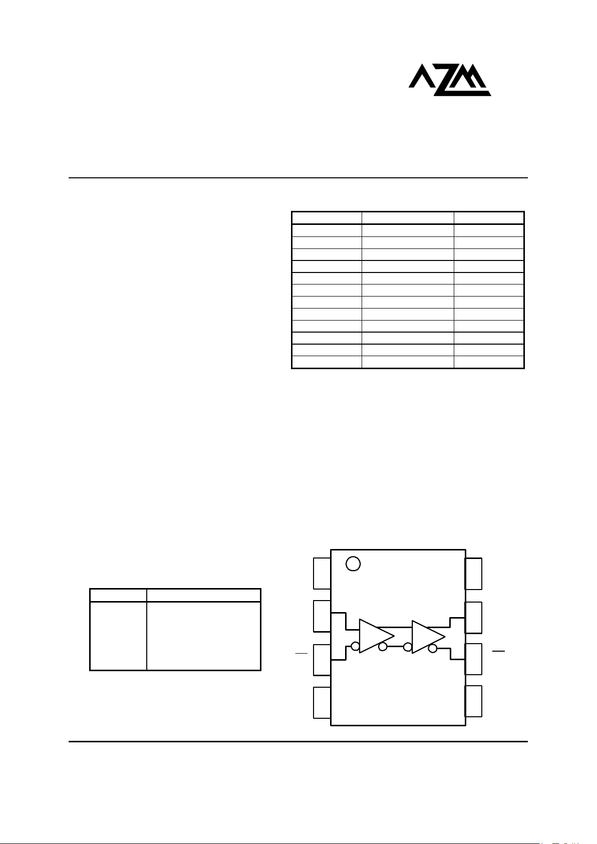
LOGIC DIAGRAM AND PINOUT ASSIGNMENT
8
5
6
7
4
3
2
1
V
CC
D
V
EE
Q
Q
V
BB
D
NC
PACKAGE AVAILABILITY
PACKAGE PART NO. MARKING
SOIC 8 AZ10EP16D AZM10EP16
SOIC 8 T&R AZ10EP16DR1 AZM10EP16
SOIC 8 T&R AZ10EP16DR2 AZM10EP16
SOIC 8 AZ100EP16D AZM100EP16
SOIC 8 T&R AZ100EP16DR1 AZM100EP16
SOIC 8 T&R AZ100EP16DR2 AZM100EP16
TSSOP 8 AZ10EP16T AZTEP16
TSSOP 8 T&R AZ10EP16TR1 AZTEP16
TSSOP 8 T&R AZ10EP16TR2 AZTEP16
TSSOP 8 AZ100EP16T AZHEP16
TSSOP 8 T&R AZ100EP16TR1 AZHEP16
TSSOP 8 T&R AZ100EP16TR2 AZHEP16
PIN DESCRIPTION
PIN FUNCTION
D, D¯ Data Inputs
Q, Q¯ Data Outputs
VBB Reference Voltage Output
V
CC
Positive Supply
V
EE
Negative Supply
NC No Connect
Page 2

AZ10EP16
AZ100EP16
March 2002 * REV - 4 www.azmicrotek.com
2
Absolute Maximum Ratings are those values beyond which device life may be impaired.
Symbol Characteristic Rating Unit
VCC PECL Power Supply (VEE = 0V) 0 to +4.5 Vdc
VI PECL Input Voltage (V
EE
= 0V) 0 to +4.5 Vdc
VEE ECL Power Supply (VCC = 0V) -4.5 to 0 Vdc
VI ECL Input Voltage (VCC = 0V) -4.5 to 0 Vdc
I
OUT
Output Current --- Continuous
--- Surge
50
100
mA
TA Operating Temperature Range -40 to +85
°C
T
STG
Storage Temperature Range -65 to +150
°C
10K ECL DC Characteristics (VEE = -3.0V to -3.6V, VCC = GND)
-40°C 0°C 25°C 85°C
Symbol Characteristic
Min Typ Max Min Typ Max Min Typ Max Min Typ Max
Unit
VOH Output HIGH Voltage1 -1135 -885 -1070 -945 -820 -1010 -760 mV
VOL Output LOW Voltage1 -1935 -1685 -1870 -1745 -1620 -1810 -1560 mV
VIH Input HIGH Voltage -1200 -885 -1150 -820 -1090 -760 mV
VIL Input LOW Voltage -1935 -1530 -1870 -1450 -1810 -1410 mV
VBB Reference Voltage -1430 -1300 -1380 -1270 -1350 -1250 -1310 -1190 mV
IIH
Input HIGH Current 175 175 175 175
µA
IIL
Input LOW Current
D
D¯
0.5
-150
0.5
-150
0.5
-150
0.5
-150
µA
IEE Power Supply Current 20 25 33 21 26 34 21 27 35 23 29 37 mA
1. Each output is terminated through a 50Ω resistor to VCC – 2V.
10K LVPECL DC Characteristics (VEE = GND, VCC = +3.3V)
-40°C 0°C 25°C 85°C
Symbol Characteristic
Min T
yp
Max Min T
yp
Max Min T
yp
Max Min T
yp
Max
Unit
VOH Output HIGH Voltage
1,2
2165 2415 2230 2355 2480 2290 2540 mV
VOL Output LOW Voltage
1,2
1365 1615 1430 1555 1680 1490 1740 mV
VIH Input HIGH Voltage1 2100 2415 2035 2480 2210 2540 mV
VIL Input LOW Voltage1 1365 1770 1430 1850 1490 1890 mV
VBB Reference Voltage1 1870 2000 1920 2030 1950 2050 1990 2110 mV
IIH Input HIGH Current 175 175 175 175
µA
IIL
Input LOW Current
D
D¯
0.5
-150
0.5
-150
0.5
-150
0.5
-150
µA
IEE Power Supply Current 20 25 33 21 26 34 21 27 35 23 29 37 mA
1. For supply voltages other that 3.3V, use the ECL table values and ADD supply voltage value.
2. Each output is terminated through a 50Ω resistor to V
CC
– 2V.
100K ECL DC Characteristics (V
EE
= -3.0V to -3.6V, VCC = GND)
-40°C 0°C 25°C 85°C
Symbol Characteristic
Min Typ Max Min Typ Max Min Typ Max Min Typ Max
Unit
VOH Output HIGH Voltage1 -1085 -880 -1025 -880 -1025 -955 -880 -1025 -880 mV
VOL Output LOW Voltage1 -1830 -1555 -1810 -1620 -1810 -1705 -1620 -1810 -1620 mV
VIH Input HIGH Voltage -1220 -880 -1160 -880 -1160 -880 -1160 -880 mV
VIL Input LOW Voltage -1830 -1540 -1810 -1480 -1810 -1480 -1810 -1480 mV
VBB Reference Voltage -1440 -1320 -1380 -1260 -1380 -1260 -1380 -1260 mV
IIH
Input HIGH Current 175 175 175 175
µA
IIL
Input LOW Current
D
D¯
0.5
-150
0.5
-150
0.5
-150
0.5
-150
µA
IEE Power Supply Current 19 24 32 20 25 33 21 26 35 23 29 38 mA
1. Each output is terminated through a 50Ω resistor to VCC – 2V.
Page 3

AZ10EP16
AZ100EP16
March 2002 * REV - 4 www.azmicrotek.com
3
100K LVPECL DC Characteristics (V
EE
= GND, VCC = +3.3V)
-40°C 0°C 25°C 85°C
Symbol Characteristic
Min T
yp
Max Min T
yp
Max Min T
yp
Max Min T
yp
Max
Unit
VOH Output HIGH Voltage
1,2
2215 2420 2275 2420 2275 2345 2420 2275 2420 mV
VOL Output LOW Voltage
1,2
1470 1745 1490 1680 1490 1595 1680 1490 1680 mV
VIH Input HIGH Voltage1 2080 2420 2140 2420 2140 2420 2140 2420 mV
VIL Input LOW Voltage1 1470 1760 1490 1820 1490 1820 1490 1820 mV
VBB Reference Voltage1 1860 1980 1920 2040 1920 2040 1920 2040 mV
IIH Input HIGH Current 175 175 175 175
µA
IIL
Input LOW Current
D
D¯
0.5
-150
0.5
-150
0.5
-150
0.5
-150
µA
IEE Power Supply Current 19 24 32 20 25 33 21 26 35 23 29 38 mA
1. For supply voltages other that 3.3V, use the ECL table values and ADD supply voltage value.
2. Each output is terminated through a 50Ω resistor to V
CC
– 2V.
AC Characteristics (VEE = -3.0 to -3.6V, VCC = GND or VEE = GND, VCC = +3.0V to +3.6V)
-40°C 0°C 25°C 85°C
Symbol Characteristic
Min Typ Max Min Typ Max Min Typ Max Min Typ Max
Unit
f
max
Maximum Toggle
Frequency
4
>4 >4 >4 >4 GHz
t
PLH
/ t
PHL
Input to
Output Delay
(DIFF) 100 160 240 100 160 240 100 160 240 120 190 280 ps
t
SKEW
Duty Cycle Skew1 (Diff) 5 5 20 5 20 5 20 ps
V
PP
(AC) Minimum Input Swing2 150 150 150 150 mV
V
CMR
Common Mode Range3
V
EE
+
2.0
V
CC
V
EE
+
2.0
V
CC
V
EE
+
2.0
V
CC
V
EE
+
2.0
V
CC
V
tr / tf
Output Rise/Fall Times Q
(20% - 80%)
120 170 130 180 130 180 150 200 ps
1. Duty cycle skew is the difference between a t
PLH
and t
PHL
propagation delay through a device.
2. V
PP
is the minimum peak-to-peak differential input swing for which AC parameters are guaranteed.
3. The V
CMR
range is referenced to the most positive side of the differential input signal. Normal operation is obtained if the HIGH level falls within
the specified range and the peak-to-peak voltage lies between V
PP
(min) and 1V.
4. See Graph Below.
Large Signal Performance*
0
100
200
300
400
500
600
700
800
900
0 1000 2000 3000 4000 5000 6000
FREQUENCY (MHz)
V
OUTpp
(mV)
*Measured using a 750mV differential input source at 50% duty cycle.
Page 4

AZ10EP16
AZ100EP16
March 2002 * REV - 4 www.azmicrotek.com
4
MILLIMETERS INCHES
DIM
MIN MAX MIN MAX
A
1.75 0.069
A1
0.10 0.25 0.004 0.010
A2
1.25 1.45 0.049 0.057
A3
0.25 0.01
bp
0.36 0.49 0.014 0.019
c
0.19 0.25 0.0075 0.0100
D
4.8 5.0 0.19 0.20
E
3.8 4.0 0.15 0.16
e
1.27 0.050
HE
5.80 6.20 0.228 0.244
L
1.05 0.041
Lp
0.40 1.00 0.016 0.039
Q
0.60 0.70 0.024 0.028
v
0.25 0.01
w
0.25 0.01
y
0.10 0.004
Z
0.30 0.70 0.012 0.028
θ
0
O
8
O
0
O
8
O
N
OTES:
1. DIMENSIONS D AND E DO NOT
INCLUDE MOLD PROTRUSION.
2. MAXIMUM MOLD PROTRUSION
FOR D IS 0.15mm.
3. MAXIMUM MOLD PROTRUSION
FOR E IS 0.25mm.
PACKAGE DIAGRAM
SOIC 8
Page 5

AZ10EP16
AZ100EP16
March 2002 * REV - 4 www.azmicrotek.com
5
PACKAGE DIAGRAM
TSSOP 8
MILLIMETERS
DIM
MIN MAX
A
1.10
A1
0.05 0.15
A2
0.80 0.95
A3
0.25
bp
0.25 0.45
c
0.15 0.28
D
2.90 3.10
E
2.90 3.10
e
0.65
HE
4.70 5.10
L
0.94
Lp
0.40 0.70
v
0.10
w
0.10
y
0.10
Z
0.35 0.70
θ
0
O
6
O
N
OTES:
1. DIMENSIONS D AND E DO NOT
INCLUDE MOLD PROTRUSION.
2. MAXIMUM MOLD PROTRUSION
FOR D IS 0.15mm.
3. MAXIMUM MOLD PROTRUSION
FOR E IS 0.25mm.
Page 6

AZ10EP16
AZ100EP16
March 2002 * REV - 4 www.azmicrotek.com
6
Arizona Microtek, Inc. reserves the right to change circuitry and specifications at any time without prior notice. Arizona Microtek, Inc.
makes no warranty, representation or guarantee regarding the suitability of its products for any particular purpose, nor does Arizona
Microtek, Inc. assume any liability arising out of the application or use of any product or circuit and specifically disclaims any and all
liability, including without limitation special, consequential or incidental damages. Arizona Microtek, Inc. does not convey any license
rights nor the rights of others. Arizona Microtek, Inc. products are not designed, intended or authorized for use as components in systems
intended to support or
sustain life, or for any other application in which the failure of the Arizona Microtek, Inc. product could create a
situation where personal injury or death may occur. Should Buyer purchase or use Arizona Microtek, Inc. products for any such
unintended or unauthorized application, Buyer shall indemnify and hold Arizona Microtek, Inc. and its officers,
employees, subsidiaries,
affiliates, and distributors harmless against all claims, costs, damages, and expenses, and reasonable attorney fees arising out of, directly
or indirectly, any claim of personal injury or death associated with such unintended
or unauthorized use, even if such claim alleges tha
t
Arizona Microtek, Inc. was negligent regarding the design or manufacture of the part.
 Loading...