

Datasheet AZ10ELT22TR2, AZ10ELT22TR1, AZ10ELT22T, AZ10ELT22DR2, AZ10ELT22DR1 Datasheet (AZMIC)
...Page 1
AZ10ELT22
AZ100ELT22
Dual CMOS/TTL to Differential PECL Translator
1630 S. STAPLEY DR., SUITE 125 • MESA, ARIZONA 85204 • USA • (480) 962-5881 • FAX (480) 890-2541
www.azmicrotek.com
ARIZONA MICROTEK, INC.
FEATURES
• 0.5ns Typical Propagation Delay
• <100ps Typical Output to Output Skew
• Differential PECL Outputs
• Flow Through Pinouts
• Operating Range of 3.0V to 5.5V
• Direct Replacement for ON Semiconductor
MC10ELT22 & MC100ELT22
DESCRIPTION
The AZ10/100ELT22 is a dual CMOS/TTL to differential PECL translator. Because PECL (Positive ECL)
levels are used, only V
CC
and ground are required. The small outline packaging and the low skew, dual gate design
of the ELT22 makes it ideal for applications that require the translation of a clock and a data signal.
The ELT22 is available in both PECL standards: the 10ELT is compatible with PECL 10K logic levels while
the 100ELT is compatible with PECL 100K logic levels.
NOTE: Specifications in PECL tables are valid when thermal equilibrium is established.
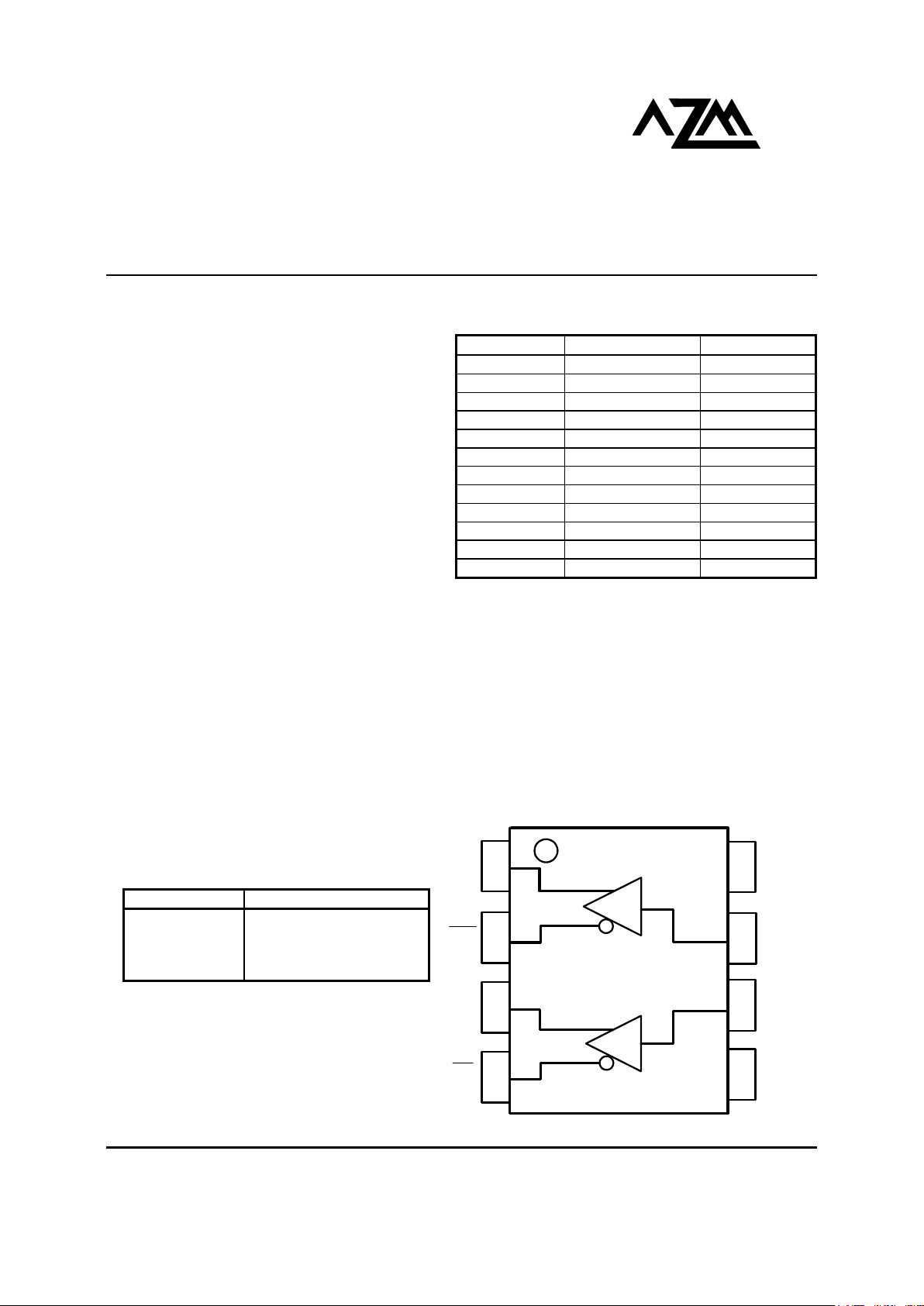
LOGIC DIAGRAM AND PINOUT ASSIGNMENT
8
5
6
7
4
3
2
1
V
CC
D0
GND
Q0
Q0
Q1
Q1
D1
PECL
TTL/
CMOS
PACKAGE AVAILABILITY
PACKAGE PART NO. MARKING
SOIC 8 AZ10ELT22D AZM10ELT22
SOIC 8 T&R AZ10ELT22DR1 AZM10ELT22
SOIC 8 T&R AZ10ELT22DR2 AZM10ELT22
SOIC 8 AZ100ELT22D AZM100ELT22
SOIC 8 T&R AZ100ELT22DR1 AZM100ELT22
SOIC 8 T&R AZ100ELT22DR2 AZM100ELT22
TSSOP 8 AZ10ELT22T AZTLT22
TSSOP 8 T&R AZ10ELT22TR1 AZTLT22
TSSOP 8 T&R AZ10ELT22TR2 AZTLT22
TSSOP 8 AZ100ELT22T AZHLT22
TSSOP 8 T&R AZ100ELT22TR1 AZHLT22
TSSOP 8 T&R AZ100ELT22TR2 AZHLT22
PIN DESCRIPTION
PIN FUNCTION
Q0, Q0¯¯ - Q1, Q1¯¯ Differential PECL Outputs
D0, D1 CMOS/TTL Input
VCC Positive Supply
GND Ground
Page 2
AZ10ELT22
AZ100ELT22
April 2002 * REV - 3 www.azmicrotek.com
2
Absolute Maximum Ratings are those values beyond which device life may be impaired.
Symbol Characteristic Value Unit
VCC DC Supply Voltage (Referenced to GND) 8.0 V
VIN Input Voltage 0 to 6.0 V
I
OUT
Current Applied to Output in Low Output State ---Continuous
---Surge
50
100
mA
TA Operating Temperature Range (In Free-Air) -40 to +85
°C
T
STG
Storage Temperature Range -65 to +150
°C
TTL/CMOS INPUT DC CHARACTERISTICS (GND = 0.0V, VCC = +3.0V to +5.5V)
Symbol Characteristic Min Typ Max Unit Condition
IIH Input HIGH Current 15
µA
VIN = 2.7V
IIH Input HIGH Current 20
µA
VIN = VCC
IIL Input LOW Current -0.1 mA VIN = 0.5V
VIK Input Clamp Diode Voltage -1.2 V IIN = -18mA
VIH Input HIGH Voltage 2.0 V
VIL Input LOW Voltage 0.8 V
10K LVPECL DC Characteristics GND = 0.0V, V
CC
= +3.3V)
-40°C 0°C 25°C 85°C
Symbol Characteristic
Min T
yp
Max Min T
yp
Max Min T
yp
Max Min T
yp
Max
Unit
VOH Output HIGH Voltage
1,2
2170 2410 2245 2460 2295 2400 2490 2390 2580 mV
VOL Output LOW Voltage
1,2
1350 1685 1350 1670 1350 1550 1670 1350 1705 mV
ICC Power Supply Current
3
24 24 24 25 mA
1. Output parameters vary 1:1 with VCC.
2. Each output is terminated through a 50Ω resistor to V
CC
– 2V.
3. I
CC
measurements must be done with outputs open.
10K PECL DC Characteristics (GND = 0.0V, V
CC
= +5.0V)
-40°C 0°C 25°C 85°C
Symbol Characteristic
Min T
yp
Max Min T
yp
Max Min T
yp
Max Min T
yp
Max
Unit
VOH Output HIGH Voltage
1,2
3870 4110 3945 4160 3995 4100 4190 4090 4280 mV
VOL Output LOW Voltage
1,2
3050 3385 3050 3370 3050 3250 3370 3050 3405 mV
ICC Power Supply Current
3
24 24 24 25 mA
1. Output parameters vary 1:1 with VCC.
2. Each output is terminated through a 50Ω resistor to V
CC
– 2V.
3. I
CC
measurements must be done with outputs open.
100K LVPECL DC Characteristics (GND = 0.0V, V
CC
= +3.3V)
-40°C 0°C 25°C 85°C
Symbol Characteristic
Min T
yp
Max Min T
yp
Max Min T
yp
Max Min T
yp
Max
Unit
VOH Output HIGH Voltage
1,2
2160 2420 2205 2420 2235 2345 2420 2255 2420 mV
VOL Output LOW Voltage
1,2
1470 1745 1490 1680 1490 1595 1680 1490 1680 mV
ICC Power Supply Current
3
24 24 24 25 mA
1. Output parameters vary 1:1 with VCC.
2. Each output is terminated through a 50Ω resistor to V
CC
– 2V.
3. I
CC
measurements must be done with outputs open.
100K PECL DC Characteristics (GND = 0.0V, V
CC
= +5.0V)
-40°C 0°C 25°C 85°C
Symbol Characteristic
Min T
yp
Max Min T
yp
Max Min T
yp
Max Min T
yp
Max
Unit
VOH Output HIGH Voltage
1,2
3860 4120 3905 4120 3935 4045 4120 3955 4120 mV
VOL Output LOW Voltage
1,2
3170 3445 3190 3380 3190 3295 3380 3190 3380 mV
ICC Power Supply Current
3
24 24 24 25 mA
1. Output parameters vary 1:1 with VCC.
2. Each output is terminated through a 50Ω resistor to V
CC
– 2V.
3. I
CC
measurements must be done with outputs open.
Page 3

AZ10ELT22
AZ100ELT22
April 2002 * REV - 3 www.azmicrotek.com
3
AC Characteristics (GND = 0.0V, V
CC
= +3.0V to +5.5V)
-400C
0°C 25°C 85°C
Unit Condition
Symbol Characteristic
Min Max Min Max Min Typ Max Min Max
t
PLH
Propagation Delay1 0.2 0.7 0.2 0.7 0.2 0.4 0.7 0.2 0.7 ns
t
PHL
Propagation Delay1 0.2 0.7 0.2 0.7 0.2 0.4 0.7 0.2 0.7 ns
tr/tf Output Rise/Fall Time 0.25 0.7 0.25 0.7 0.25 0.7 0.25 0.7 ns 20-80%
f
MAX
Maximum Frequency2 350 350 350 350 MHz
f
MAX
Maximum Frequency3 670 800 800 800 MHz
1. Propagation delay is measured from +1.5V on the input to 50% of the PECL output swing. Input rise/fall times are < 1ns/V.
2. Full swing PECL output.
3. Output at –3 dB
Large Signal Performance
150
250
350
450
550
650
750
850
1 10 100 1000 10000
Frequency (MHz)
Single ended Output (mV p-p)
Input: 150 mV p-p Sine
Wave Single Ended
Page 4

AZ10ELT22
AZ100ELT22
April 2002 * REV - 3 www.azmicrotek.com
4
MILLIMETERS INCHES
DIM
MIN MAX MIN MAX
A
1.35 1.75 .053 0.069
A1
0.10 0.25 0.004 0.010
A2
1.28 1.57 0.050 0.062
A3
0.25 0.01
bp
0.36 0.49 0.014 0.019
c
0.19 0.25 0.0075 0.0100
D
4.80 5.00 0.19 0.20
E
3.80 4.00 0.15 0.16
e
1.27 0.050
HE
5.80 6.20 0.228 0.244
L
1.05 0.041
Lp
0.40 1.27 0.016 0.050
Q
0.60 0.70 0.024 0.028
v
0.25 0.01
w
0.25 0.01
y
0.10 0.004
Z
0.30 0.70 0.012 0.028
θ
0
O
8
O
0
O
8
O
N
OTES:
1. DIMENSIONS D AND E DO NOT
INCLUDE MOLD PROTRUSION.
2. MAXIMUM MOLD PROTRUSION
FOR D IS 0.15mm.
3. MAXIMUM MOLD PROTRUSION
FOR E IS 0.25mm.
PACKAGE DIAGRAM
SOIC 8
Page 5

AZ10ELT22
AZ100ELT22
April 2002 * REV - 3 www.azmicrotek.com
5
PACKAGE DIAGRAM
TSSOP 8
MILLIMETERS
DIM
MIN MAX
A
1.10
A1
0.05 0.15
A2
0.75 0.95
A3
0.25
bp
0.22 0.40
c
0.13 0.23
D
2.90 3.10
E
2.90 3.10
e
0.65
HE
4.75 5.05
L
0.95
Lp
0.40 0.70
v
0.10
w
0.08
y
0.10
Z
0.38 0.64
θ
0
O
6
O
N
OTES:
1. DIMENSIONS D AND E DO NOT
INCLUDE MOLD PROTRUSION.
2. MAXIMUM MOLD PROTRUSION
FOR D IS 0.15mm.
3. MAXIMUM MOLD PROTRUSION
FOR E IS 0.25mm.
Page 6

AZ10ELT22
AZ100ELT22
April 2002 * REV - 3 www.azmicrotek.com
6
Arizona Microtek, Inc. reserves the right to change circuitry and specifications at any time without prior notice. Arizona Microtek, Inc.
makes no warranty, representation or guarantee regarding the suitability of its products for any particular purpose, nor does Arizona
Microtek, Inc. assume any liability arising out of the application or use of any product or circuit and specifically disclaims any and all
liability, including without limitation special, consequential or incidental damages. Arizona Microtek, Inc. does not convey any license
rights nor the rights of others. Arizona Microtek, Inc. products are not designed, intended or authorized for use as components in systems
intended to support or sustain life, or for any other application in which the failure of the Arizona Microtek, Inc. product could create a
situation where personal injury or death may occur. Should Buyer purchase or use Arizona Microtek, Inc. products for any such
unintended or unauthorized application, Buyer shall indemnify and hold Arizona Microtek, Inc. and its officers, employees, subsidiaries,
affiliates, and distributors harmless against all claims, costs, damages, and expenses, and reasonable attorney fees arising out of, directly
or indirectly, any claim of personal injury or death associated with such unintended or unauthorized use, even if such claim alleges tha
t
Arizona Microtek, Inc. was negligent regarding the design or manufacture of the part.
 Loading...