

Datasheet AZ10EL11TR2, AZ10EL11TR1, AZ10EL11T, AZ10EL11DR2, AZ10EL11DR1 Datasheet (AZMIC)
...Page 1
AZ10EL11
AZ100EL11
ECL/PECL 1:2 Differential Fanout Buffer
ARIZONA MICROTEK, INC.
FEATURES
• 265ps Propagation Delay
• 5ps Skew Between Outputs
• High Bandwidth Output Transitions
• 75kΩ Internal Input Pulldown Resistors
• Direct Replacement for ON Semiconductor
MC10EL11 & MC100EL11
PACKAGE PART NO. MARKING
SOIC 8 AZ10EL11D AZM10EL11
SOIC 8 T&R AZ10EL11DR1 AZM10EL11
SOIC 8 T&R AZ10EL11DR2 AZM10EL11
SOIC 8 AZ100EL11D AZM100EL11
SOIC 8 T&R AZ100EL11DR1 AZM100EL11
SOIC 8 T&R AZ100EL11DR2 AZM100EL11
TSSOP 8 AZ10EL11T AZTEL11
TSSOP 8 T&R AZ10EL11TR1 AZTEL11
TSSOP 8 T&R AZ10EL11TR2 AZTEL11
TSSOP 8 AZ100EL11T AZHEL11
TSSOP 8 T&R AZ100EL11TR1 AZHEL11
TSSOP 8 T&R AZ100EL11TR2 AZHEL11
PACKAGE AVAILABILITY
DESCRIPTION
The AZ10/100EL11 is a differential 1:2 fanout gate. The device is functionally similar to the E111 device but
with higher performance capabilities. Having within-device skews and output transition times significantly
improved over the E111, the EL11 is ideally suited for those applications that require the ultimate in AC
performance.
The differential inputs of the EL11 employ clamping circuitry to maintain stability under open input conditions.
If the inputs are left open (pulled to V
NOTE: Specifications in the ECL/PECL tables are valid when thermal equilibrium is established.
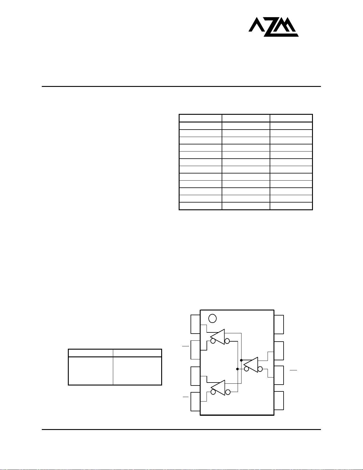
D, D¯ Data Inputs
Q0, Q0¯¯, Q1, Q1¯¯ Data Outputs
V
V
PIN DESCRIPTION
PIN FUNCTION
CC
EE
Positive Supply
Negative Supply
) the Q outputs will go LOW.
EE
LOGIC DIAGRAM AND PINOUT ASSIGNMENT
1
Q0
Q0
2
Q1
3
Q1
4
8
7
6
5
V
CC
D
D
V
EE
1630 S. STAPLEY DR., SUITE 125 • MESA, ARIZONA 85204 • USA • (480) 962-5881 • FAX (480) 890-2541
www.azmicrotek.com
Page 2
AZ10EL11
yp
yp
yp
yp
yp
yp
yp
yp
AZ100EL11
Absolute Maximum Ratings are those values beyond which device life may be impaired.
Symbol Characteristic Rating Unit
VCC PECL Power Supply (VEE = 0V) 0 to +8.0 Vdc
VI PECL Input Voltage (V
= 0V) 0 to +6.0 Vdc
EE
VEE ECL Power Supply (VCC = 0V) -8.0 to 0 Vdc
VI ECL Input Voltage (VCC = 0V) -6.0 to 0 Vdc
I
OUT
Output Current --- Continuous
--- Surge
50
100
TA Operating Temperature Range -40 to +85
T
STG
Storage Temperature Range -65 to +150
10K ECL DC Characteristics (VEE = -4.75V to -5.5V, VCC = GND)
Symbol Characteristic
VOH Output HIGH Voltage1 -1080 -890 -1020 -840 -980 -810 -910 -720 mV
VOL Output LOW Voltage1 -1950 -1650 -1950 -1630 -1950 -1630 -1950 -1595 mV
VIH Input HIGH Voltage -1230 -890 -1170 -840 -1130 -810 -1060 -720 mV
VIL Input LOW Voltage -1950 -1500 -1950 -1480 -1950 -1480 -1950 -1445 mV
IIH
IIL
Input HIGH Current 150 150 150 150
Input LOW Current 0.5 0.5 0.5 0.5
IEE Power Supply Current 26 31 26 31 26 31 26 31 mA
1. Each output is terminated through a 50Ω resistor to V
-40°C 0°C 25°C 85°C
Min Typ Max Min Typ Max Min Typ Max Min Typ Max
– 2V.
CC
10K PECL DC Characteristics (VEE = GND, VCC = +5.0V)
Symbol Characteristic
VOH Output HIGH Voltage
VOL Output LOW Voltage
1,2
3920 4110 3980 4160 4020 4190 4090 4280 mV
1,2
3050 3350 3050 3370 3050 3370 3050 3405 mV
VIH Input HIGH Voltage1 3770 4110 3830 4160 3870 4190 3940 4280 mV
VIL Input LOW Voltage1 3050 3500 3050 3520 3050 3520 3050 3555 mV
IIH Input HIGH Current 150 150 150 150
IIL
Input LOW Current 0.5 0.5 0.5 0.5
IEE Power Supply Current 26 31 26 31 26 31 26 31 mA
1. For supply voltages other that 5.0V, use the ECL table values and ADD supply voltage value.
2. Each output is terminated through a 50Ω resistor to V
-40°C 0°C 25°C 85°C
Min T
Max Min T
– 2V.
CC
Max Min T
100K ECL DC Characteristics (V
Symbol Characteristic
VOH Output HIGH Voltage1 -1085 -1005 -880 -1025 -955 -880 -1025 -955 -880 -1025 -955 -880 mV
VOL Output LOW Voltage1 -1830 -1695 -1555 -1810 -1705 -1620 -1810 -1705 -1620 -1810 -1705 -1620 mV
VIH Input HIGH Voltage -1165 -880 -1165 -880 -1165 -880 -1165 -880 mV
VIL Input LOW Voltage -1810 -1475 -1810 -1475 -1810 -1475 -1810 -1475 mV
IIH
IIL
IEE Power Supply Current 26 31 26 31 26 31 30 36 mA
1. Each output is terminated through a 50Ω resistor to V
Input HIGH Current 150 150 150 150
Input LOW Current 0.5 0.5 0.5 0.5
= -4.2V to -5.5V, VCC = GND)
EE
-40°C 0°C 25°C 85°C
Min Typ Max Min Typ Max Min Typ Max Min Typ Max
– 2V.
CC
100K PECL DC Characteristics (VEE = GND, VCC = +5.0V)
Symbol Characteristic
VOH Output HIGH Voltage
VOL Output LOW Voltage
1,2
3915 3995 4120 3975 4045 4120 3975 4045 4120 3975 4045 4120 mV
1,2
3170 3305 3445 3190 3295 3380 3190 3295 3380 3190 3295 3380 mV
VIH Input HIGH Voltage1 3835 4120 3835 4120 3835 4120 3835 4120 mV
VIL Input LOW Voltage1 3190 3525 3190 3525 3190 3525 3190 3525 mV
IIH Input HIGH Current 150 150 150 150
IIL
Input LOW Current 0.5 0.5 0.5 0.5
IEE Power Supply Current 26 31 26 31 26 31 30 36 mA
1. For supply voltages other that 5.0V, use the ECL table values and ADD supply voltage value.
2. Each output is terminated through a 50Ω resistor to V
-40°C 0°C 25°C 85°C
Min T
Max Min T
– 2V.
CC
Max Min T
Max Min T
Max Min T
mA
°C
°C
Max
Max
Unit
µA
µA
Unit
µA
µA
Unit
µA
µA
Unit
µA
µA
October 2001 * REV - 2 www.azmicrotek.com
2
Page 3

AZ10EL11
AZ100EL11
AC Characteristics (V
=10E(-4.75V to -5.5V), 100E(-4.2V to -5.5V); VCC =GND or VEE =GND; VCC =10E(+4.75V to +5.5V),
EE
100E(+4.2V to +5.5V))
Symbol Characteristic
t
PLH
t
SKEW
V
PP
V
CMR
tr / tf
Propagation Delay to
/ t
PHL
Output
Within-Device Skew
Duty Cycle Skew
1
2
(AC) Minimum Input Swing3 150 150 150 150 mV
Common Mode Range4
Rise/Fall Time
20 – 80%
1. Within-device skew defined as identical transitions on similar paths through a device.
2. Duty cycle skew is the difference between a t
is the minimum peak-to-peak differential input swing for which AC parameters are guaranteed. The device has a DC voltage gain of ≈ 40.
3. V
PP
4. The V
range is referenced to the most positive side of the differential input signal. Normal operation is obtained if the HIGH level falls within
CMR
the specified range and the peak-to-peak voltage lies between V
-40°C 0°C 25°C 85°C
Min Typ Max Min Typ Max Min Typ Max Min Typ Max
Unit
135 260 385 185 260 335 190 265 340 215 290 365 ps
V
CC
2.0
5
5
-
V
-
VCC -
CC
0.4
2.0
5
20
5
20
-
VCC -
V
CC
0.4
2.0
5
20
5
20
-
VCC -
V
CC
0.4
2.0
5
20
5
20
-
V
CC
0.4
100 350 100 350 100 350 100 350 ps
and t
PLH
propagation delay through a device.
PHL
(min) and 1V.
PP
ps
V
October 2001 * REV - 2 www.azmicrotek.com
3
Page 4

AZ10EL11
N
AZ100EL11
PACKAGE DIAGRAM
SOIC 8
MILLIMETERS INCHES
OTES:
1. DIMENSIONS D AND E DO NOT
INCLUDE MOLD PROTRUSION.
2. MAXIMUM MOLD PROTRUSION
FOR D IS 0.15mm.
3. MAXIMUM MOLD PROTRUSION
FOR E IS 0.25mm.
DIM
A
A1
A2
A3
bp
c
D
E
e
HE
L
Lp
Q
v
w
y
Z
θ
MIN MAX MIN MAX
1.75 0.069
0.10 0.25 0.004 0.010
1.25 1.45 0.049 0.057
0.25 0.01
0.36 0.49 0.014 0.019
0.19 0.25 0.0075 0.0100
4.8 5.0 0.19 0.20
3.8 4.0 0.15 0.16
1.27 0.050
5.80 6.20 0.228 0.244
1.05 0.041
0.40 1.00 0.016 0.039
0.60 0.70 0.024 0.028
0.25 0.01
0.25 0.01
0.10 0.004
0.30 0.70 0.012 0.028
O
8
0
O
0
O
8
October 2001 * REV - 2 www.azmicrotek.com
4
O
Page 5

AZ10EL11
N
AZ100EL11
PACKAGE DIAGRAM
TSSOP 8
MILLIMETERS
OTES:
1. DIMENSIONS D AND E DO NOT
INCLUDE MOLD PROTRUSION.
2. MAXIMUM MOLD PROTRUSION
FOR D IS 0.15mm.
3. MAXIMUM MOLD PROTRUSION
FOR E IS 0.25mm.
DIM
A
A1
A2
A3
bp
D
E
HE
L
Lp
w
Z
θ
MIN MAX
1.10
0.05 0.15
0.80 0.95
0.25 0.45
c
0.15 0.28
2.90 3.10
2.90 3.10
e
4.70 5.10
0.40 0.70
v
y
0.35 0.70
O
6
0
0.25
0.65
0.94
0.10
0.10
0.10
O
October 2001 * REV - 2 www.azmicrotek.com
5
Page 6

AZ10EL11
t
AZ100EL11
Arizona Microtek, Inc. reserves the right to change circuitry and specifications at any time without prior notice. Arizona Microtek, Inc.
makes no warranty, representation or guarantee regarding the suitability of its products for any particular purpose, nor does Arizona
Microtek, Inc. assume any liability arising out of the application or use of any product or circuit and specifically disclaims any and all
liability, including without limitation special, consequential or incidental damages. Arizona Microtek, Inc. does not convey any license
rights nor the rights of others. Arizona Microtek, Inc. products are not designed, intended or authorized for use as components in systems
intended to support or sustain life, or for any other application in which the failure of the Arizona Microtek, Inc. product could create a
situation where personal injury or death may occur. Should Buyer purchase or use Arizona Microtek, Inc. products for any such
unintended or unauthorized application, Buyer shall indemnify and hold Arizona Microtek, Inc. and its officers, employees, subsidiaries,
affiliates, and distributors harmless against all claims, costs, damages, and expenses, and reasonable attorney fees arising out of, directly
or indirectly, any claim of personal injury or death associated with such unintended or unauthorized use, even if such claim alleges tha
Arizona Microtek, Inc. was negligent regarding the design or manufacture of the part.
October 2001 * REV - 2 www.azmicrotek.com
6
 Loading...